Semiconductor device with group III-V channel and group IV source-drain and method for manufacturing the same

a technology of semiconductor devices and source-drain, which is applied in the direction of semiconductor/solid-state device manufacturing, semiconductor devices, electrical apparatus, etc., can solve the problems of poor electrical properties, poor efficiency of confined carriers, and degradation of electrical properties, so as to reduce cost, enhance electrical properties, and efficient confinement

Inactive Publication Date: 2011-04-19
NAT CHIAO TUNG UNIV
View PDF7 Cites 78 Cited by
  • Summary
  • Abstract
  • Description
  • Claims
  • Application Information

AI Technical Summary

Benefits of technology

[0021]A semiconductor device with group III-V channel and group IV source-drain manufactured according to the present invention has the following advantages: (1) the problems of insufficient energy level density and doping concentration are resolved; (2) channel carriers can be efficiently confined by forming a stacked structure such as a quantum well or two-dimension electron gas or metal-oxide semiconductor; (3) the integration of the group III-V material into a silicon germanium or silicon substrate can reduce cost; and (4) the group III-V channel grown with strain can further enhance the electrical properties since the group IV source-drain, such as SixGe1-x (x=0˜1), with a relative small lattice constant can apply compressive strain to the group III-V channel, such as GaAs, with a relative large lattice constant while the group IV source-drain themselves are formed with tensile strain, wherein the compressive strain can increase electron mobility to increase current.

Problems solved by technology

In the above-mentioned method, the trench 26 is formed in the substrate and is filled with an epitaxial material functioning as a carrier channel by depositing a single epitaxial film (i.e., the epitaxial material is a single layer without structural design), so the electrical properties of the manufactured devise are susceptible to the quality of epitaxial junction and can not efficiently confine carriers.
However, for the heteroepitaxial material, the defects of the heterogeneous material may extend upward to the surface of the channel portion, resulting in degradation in electrical properties.
Therefore, this arrangement is not optimized.
Although that a group III-V material is integrated into a silicon substrate to be a logic electronic device, can efficiently enhance the electrical properties of the device, once element sizes are micronized below 22 nm, a field effect transistor using the group III-V material will confront the problems of insufficient energy level density and doping concentration.

Method used


Image

  • Semiconductor device with group III-V channel and group IV source-drain and method for manufacturing the same
  • Semiconductor device with group III-V channel and group IV source-drain and method for manufacturing the same
  • Semiconductor device with group III-V channel and group IV source-drain and method for manufacturing the same

Examples


first embodiment

[0030]A first embodiment uses a group III-V epitaxial technique to manufacture a metal-oxide semiconductor field effect transistor 1.

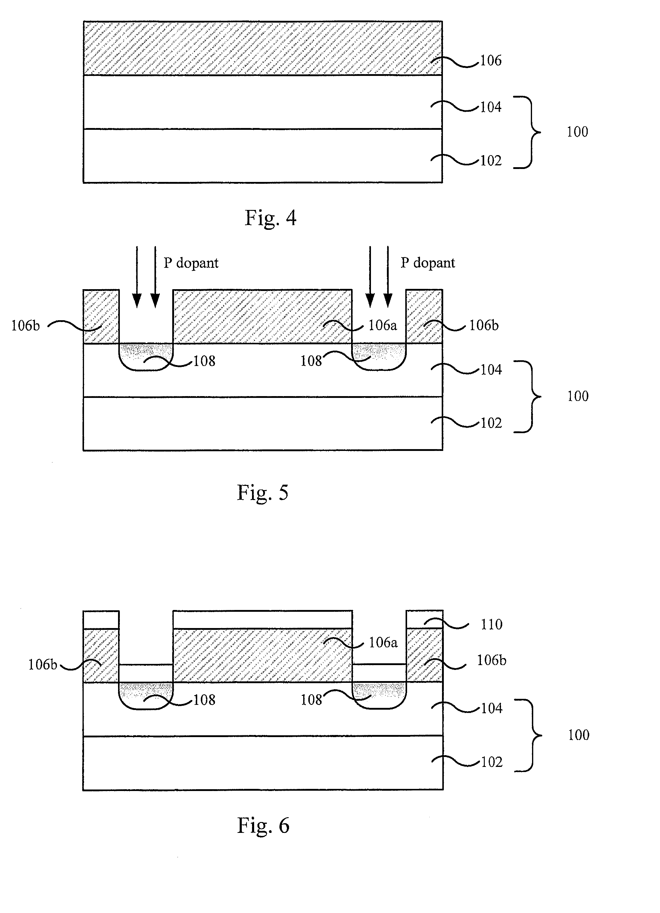
[0031]Referring to FIG. 4, a p-type silicon substrate 102 with a p-type SixGe1-x (x=0˜1) layer 104 formed thereon is prepared. Hereinafter, the p-type silicon substrate 102 together with the p-type SixGe1-x layer 104 are referred to as an SixGe1-x substrate 100. After cleaning, a first silicon dioxide layer 106 is deposited on the SixGe1-x substrate 100.

[0032]Referring to FIG. 5, a dummy gate 106a and a residual first silicon dioxide layer 106b are defined by using photolithography. The SixGe1-x substrate 100 is doped with P dopant by self-aligned ion implantation using the dummy gate 106a and the residual first silicon dioxide layer 106b as a mask, so as to form n+ source-drain 108. Referring to FIG. 6, a second silicon dioxide layer 110 is deposited to cover the entire surface. Then, the n+ source-drain 108 are activated at high temperature.

[0033]Ref...

second embodiment

[0038]A second embodiment uses a group III-V epitaxial technique to manufacture a quantum well field effect transistor (QWFET) 2.

[0039]Referring to FIG. 12, a p-type silicon substrate 202 with a p-type SixGe1-x (x=0˜1) layer 204 formed thereon is prepared. Hereinafter, the p-type silicon substrate 202 together with the p-type SixGe1-x layer 204 are referred to as an SixGe1-x substrate 200. After cleaning, a first silicon dioxide layer 206 is deposited on the SixGe1-x substrate 200.

[0040]Referring to FIG. 13, a dummy gate 206a and a residual first silicon dioxide layer 206b are defined by using photolithography. The SixGe1-x substrate 200 is doped with P dopant by self-aligned ion implantation using the dummy gate 206a and the residual first silicon dioxide layer 206b as a mask, so as to form n+ source-drain 208. Referring to FIG. 14, a second silicon dioxide layer 210 is deposited to cover the entire surface. Then, the n+ source-drain 208 are activated at high-temperature.

[0041]Refe...

third embodiment

[0046]A third embodiment uses a group III-V epitaxial technique to manufacture a high-electron-mobility transistor (HEMT) 3.

[0047]Referring to FIG. 20, a p-type silicon substrate 302 with a p-type SixGe1-x (x=0˜1) layer 304 formed thereon is prepared. Hereinafter, the p-type silicon substrate 302 together with the p-type SixGe1-x layer 304 are referred to as an SixG1-x, substrate 300. After cleaning, a first silicon dioxide layer 306 is deposited on the SixGe1-x substrate 300.

[0048]Referring to FIG. 21, a dummy gate 306a and a residual first silicon dioxide layer 306b are defined by using photolithography. The SixGei, substrate 300 is doped with P dopant by self-aligned ion implantation using the dummy gate 306a and the residual first silicon dioxide layer 306b as a mask, so as to form n+ source-drain 308. Referring to FIG. 22, a second silicon dioxide layer 310 is deposited to cover the entire surface. Then, the n+ source-drain 308 are activated at high temperature.

[0049]Referring ...


PUM


Abstract

The present invention is related to a semiconductor device with group III-V channel and group IV source-drain and a method for manufacturing the same. Particularly, the energy level density and doping concentration of group III-V materials are increased by the heteroepitaxy of group III-V and group IV materials and the structural design of elements. The method comprises: preparing a substrate; depositing a dummy gate material layer on the substrate and defining a dummy gate from the dummy gate material layer by photolithography; performing doping by self-aligned ion implantation using the dummy gate as a mask and performing activation at high temperature, so as to form source-drain; removing the dummy gate; forming a recess in the substrate between the source-drain pair by etching; forming a channel-containing stacked element in the recess by epitaxy; and forming a gate on the channel-containing stacked element.

Description

CROSS-REFERENCE TO RELATED APPLICATION[0001]This application claims all benefits accruing under 35 U.S.C. §119 from Taiwanese Patent Application No. 098140529, filed on Nov. 27, 2009 in the Intellectual Property Office Ministry of Economic Affairs, Republic of China, the disclosure of which is incorporated by reference herein.BACKGROUND OF THE INVENTION[0002]1. Field of the Invention[0003]The present invention is related to a semiconductor device with group III-V channel and group IV source-drain and a method for manufacturing a semiconductor device with group III-V channel and group IV source-drain. The method is to form a group III-V channel on a group IV substrate by epitaxy, or a group IV source-drain on a group III-V element structure by epitaxy.[0004]2. Description of the Related Art[0005]Generally, a metal-oxide-semiconductor field effect transistor (MOSFET) with very thin gate dielectrics made from silicon dioxide may experience unacceptable gate leakage currents, so the gat...

Claims


Application Information

Patent Timeline
Patent Type & Authority Patents(United States)
IPC IPC(8): H01L31/00
CPCH01L21/8258H01L29/0843H01L29/165H01L29/7783H01L29/267H01L29/66462H01L29/2003
Inventor CHANG, CHUN-YEN
Owner NAT CHIAO TUNG UNIV
Why Eureka
Try Eureka