Liquid crystal display device with an electric-field shielding layer and method of fabricating the same

a liquid crystal display and shielding layer technology, applied in static indicating devices, instruments, optics, etc., can solve the problems of defectiveness in displaying images, defectiveness called “white non-uniformity”, color non-uniformity, etc., to prevent display defectiveness, high reliability, and high quality display

Active Publication Date: 2011-05-03
NEC LCD TECH CORP
View PDF33 Cites 22 Cited by
  • Summary
  • Abstract
  • Description
  • Claims
  • Application Information

AI Technical Summary

Benefits of technology

[0045]In view of the above-mentioned problems in the conventional liquid crystal display devices, it is an object of the present invention to provide a liquid crystal display device having an opposed substrate on which on electrodes are formed, such as an in-plane switching mode liquid crystal display device, which is capable of preventing display defectiveness, in particular, color non-uniformity relative to a conventional liquid crystal display device, and presenting high-quality display and high reliability.
[0046]It is also an object of the present invention to provide such a liquid crystal display device without causing complexity in a process of fabricating a color filter and a thin film transistor.

Problems solved by technology

It is known that a twisted nematic type liquid crystal display device is accompanied with a problem of defectiveness in displaying images, caused by optical characteristics of parts constituting the liquid crystal display device or performances of liquid crystal.
For instance, as such defectiveness caused by a color filter, there is known defectiveness called “white non-uniformity”.
Apart from the above-mentioned “white non-uniformity”, there is color non-uniformity as display defectiveness, such as “red non-uniformity” and “blue non-uniformity”.
The color non-uniformity is a phenomenon in which when a light passing through one or more color layers among color layers constituting a color filter is reduced, and resultingly, a brightness of displayed color goes unbalance, and thus, displayed images are partially colored.
In particular, such color non-uniformity is likely to occur in a liquid crystal display device having an opposed substrate on which a color filter including colorants containing red, green and blue pigments at a high concentration is formed, but no electrodes are formed is.
Hence, it is not possible to prevent occurrence of color non-uniformity by the above-mentioned Japanese Patent Application Publications Nos. 2001-305332 and 2000-186225.
In Japanese Patent Application Publication No. 2002-323706, a scanning line is not shielded, resulting in that an electric field may leak from the scanning line.
However, since the electrode does not overlap the scanning line, it would not be possible to completely shield an electric field to be leaked from the scanning line.
However, since a common electrode and the transparent common electrode are formed in separate layers, it would be unavoidable for a process of fabricating an active device substrate to become complex.
As a result of the analysis having been conducted by the inventors with respect to the above-mentioned problem, color non-uniformity, it was found out that since a transparent electrode such as an electrode composed of indium tin oxide (ITO) was not formed on a surface of an opposed surface, facing a liquid crystal layer, an electric field leaking from a scanning line when liquid crystal was driven reached the opposed substrate having a color filter, and hence, the electric field was applied to color layers with the result that the color layers were electrically charged, causing display defectiveness.
As explained above, color non-uniformity in display defectiveness is caused when color layers constituting a color filter are electrically charged due to an electric field leaking from a scanning line and a signal line both formed on an active device substrate.
The electrically charged color layers cause alignment disturbance in a liquid crystal layer in a pixel area with the result of reduction in a brightness, and the reduction in a brightness cause unbalance in a desired brightness in a displayed color.
Such brightness unbalance is recognized by a viewer as color non-uniformity.

Method used


Image

  • Liquid crystal display device with an electric-field shielding layer and method of fabricating the same
  • Liquid crystal display device with an electric-field shielding layer and method of fabricating the same
  • Liquid crystal display device with an electric-field shielding layer and method of fabricating the same

Examples


first embodiment

[0100]FIG. 3 is a plan view of an active device substrate in a liquid crystal display device in accordance with the first embodiment of the present invention, FIG. 4 is a cross-sectional view taken along the line IV-IV in FIG. 3, FIG. 5A is a cross-sectional view taken along the line VA-VA in FIG. 3, and FIG. 5B is a cross-sectional view taken along the line VB-VB in FIG. 3.

[0101]Hereinbelow is explained the liquid crystal display device in accordance with the first embodiment with reference to FIGS. 3, 4, 5A and 5B.

[0102]As illustrated in FIG. 4, the liquid crystal display device is comprised of an active device substrate 31, an opposed substrate 33 arranged in facing relation to the active device substrate 31, and a liquid crystal layer 32 sandwiched between the active device substrate 31 and the opposed substrate 33.

[0103]The opposed substrate 33 is comprised of a second electrically insulating transparent substrate 35, a black matrix layer 36 formed on the second electrically in...

second embodiment

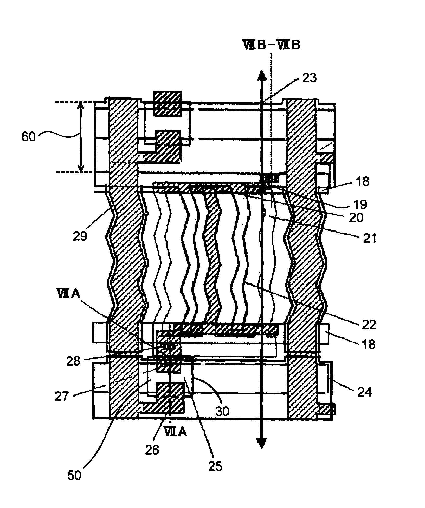
[0133]FIG. 6 is a plan view of an active device substrate in a liquid crystal display device in accordance with the second embodiment, FIG. 7A is a cross-sectional view taken along the line VIIA-VIIA in FIG. 6, and FIG. 7B is a cross-sectional view taken along the line VIIB-VIIB in FIG. 6.

[0134]Hereinbelow is explained the second embodiment with reference to FIGS. 6, 7A and 7B.

[0135]As illustrated in FIGS. 6, 7A and 7B, the electric-field shielding layer 60 in the second embodiment is designed not to have a cut-out 61. Accordingly, the liquid crystal display device in accordance with the second embodiment is structurally different from the liquid crystal display device in accordance with the first embodiment only in that the electric-field shielding layer 60 overlaps the thin film transistor 30.

[0136]Parts or elements that correspond to those of the first embodiment illustrated in FIGS. 3, 4, 5A and 5B have been provided with the same reference numerals.

[0137]The liquid crystal disp...

example 1

[0139]Example 1 corresponds to the above-mentioned first embodiment.

[0140]Hereinbelow is explained a method of fabricating a liquid crystal display device in accordance with Example 1.

[0141]First, the active device substrate 31 is fabricated as follows.

[0142]On the first electrically insulating transparent substrate 42 is formed a chromium (Cr) film having a thickness of about 280 nm as a metal layer of which the scanning line 24 and the common electrode line 18 will be comprised later. Then, the chromium film is patterned.

[0143]On the chromium film are successively deposited the first interlayer insulating film 41 comprised of a silicon nitride film having a thickness of about 400 nm, the amorphous silicon (a-Si) film 25 having a thickness of about 200 nm, and an n-type amorphous silicon film having a thickness of about 30 nm. Then, the amorphous silicon (a-Si) film 25 and the n-type amorphous silicon film are patterned into an island.

[0144]Then, a chromium (Cr) film is formed by t...


PUM

PropertyMeasurementUnit
volume resistivityaaaaaaaaaa
thicknessaaaaaaaaaa

Abstract

The liquid crystal display device includes a first substrate, a second substrate arranged in facing relation to the first substrate, and a liquid crystal layer sandwiched between the first and second substrates. The first substrate includes a thin film transistor, a pixel electrode associated with a pixel, a common electrode to which a reference voltage is applied, a data line, a scanning line, and a common electrode line. The second substrate is designed to include no electrodes thereon. The first substrate includes an electric-field shielding layer for preventing an electric field from leaking into pixels in which images are to be displayed, from the scanning line, the electric-field shielding layer being comprised of an electrically conductive layer and being formed in a layer located closer to the liquid crystal layer than an area in which the scanning line is arranged.

Description

BACKGROUND OF THE INVENTION[0001]1. Field of the Invention[0002]The invention relates to a liquid crystal display device including two substrates arranged in facing relation to each other, one of which is designed to have no electrodes thereon.[0003]2. Description of the Related Art[0004]An active matrix type liquid crystal display device including a thin film transistor (TFT) as a switch for switching on / off of pixels presents high-quality images, and hence, is used in a lot of products such as a monitor for a desk-top type computer.[0005]In general, a liquid crystal display device operates in either a twisted nematic mode in which liquid crystal molecules having twisted initial orientation are rotated vertically to transparent substrates, a VA mode in which liquid crystal molecules have initial orientation arranged vertical to substrates, or an in-plane switching (IPS) mode in which liquid crystal molecules are rotated in parallel with transparent substrates.[0006]In an in-plane s...

Claims


Application Information

Patent Timeline
Patent Type & Authority Patents(United States)
IPC IPC(8): G02F1/1343H01L29/04G09G3/36G02F1/136G02F1/133G02B5/20G02F1/1335G02F1/1339G02F1/1362G02F1/1368
CPCG02F1/134363G02F2001/136218G02F1/136218G02F1/1343
Inventor TAKAHASHI, SOUNOSUKEOKAMOTO, MAMORUNISHIDA, SHINICHI
Owner NEC LCD TECH CORP
Why Eureka
Try Eureka