Semiconductor device packaging using etched leadfingers

a technology of etching and leadfingers, which is applied in the direction of semiconductor devices, semiconductor/solid-state device details, electrical apparatus, etc., can solve the problems of insufficient signal integrity, durability, reliability, package density and cost-savings, and insufficient use of conventional integrated circuit packaging techniques in increasing numbers of modern applications. , to achieve the effect of increasing durability and reliability, increasing signal integrity, and increasing packaging density

Active Publication Date: 2011-05-10
MONTEREY RES LLC
View PDF13 Cites 17 Cited by
  • Summary
  • Abstract
  • Description
  • Claims
  • Application Information

AI Technical Summary

Benefits of technology

[0009]Accordingly, a need exists for semiconductor device packages with increased signal integrity. A need also exists for semiconductor device packages with increased durability and reliability. Additionally, a need exists for semiconductor device packages with higher packaging density and reduced cost. Embodiments of the present invention provide novel solutions to these needs and others as described below.

Problems solved by technology

Further, applications often incorporate large numbers of integrated circuits, thereby demanding high packaging density to enable placement of a larger number of integrated circuits in a given circuit board area.
Given these more demanding requirements, conventional integrated circuit packaging techniques are proving inadequate for an increasing number of modern applications.
In particular, conventional wire-bonded and flip-chip configurations fail to provide adequate signal integrity, durability, reliability, package density and cost-savings.
Although wire-bonded semiconductor device packages (e.g., 100) were widely used for some time, their use in modern applications is more limited.
Wire bonding provides poor signal integrity given long signal paths providing higher inductance, increased crosstalk, and more limited slew rates.
Reflections produced by impedance mismatches of the wire bonding further reduce signal integrity.
Further, the durability and reliability associated with wire bonding is insufficient for modern applications.
Creation of a device with a flip-chip pad arrangement adds significant cost given the design and manufacture of a new device.
Rerouting signal paths of a reoriented device with a wire-bonded pad arrangement also adds cost, while introducing the same signal integrity, reliability and durability problems present in traditional wire-bonded device packages (e.g., 100).
Further, rerouting signal paths often leads to longer and unequal-length signal paths, thereby exacerbating the signal integrity problems.

Method used


Image

  • Semiconductor device packaging using etched leadfingers
  • Semiconductor device packaging using etched leadfingers
  • Semiconductor device packaging using etched leadfingers

Examples


Embodiment Construction

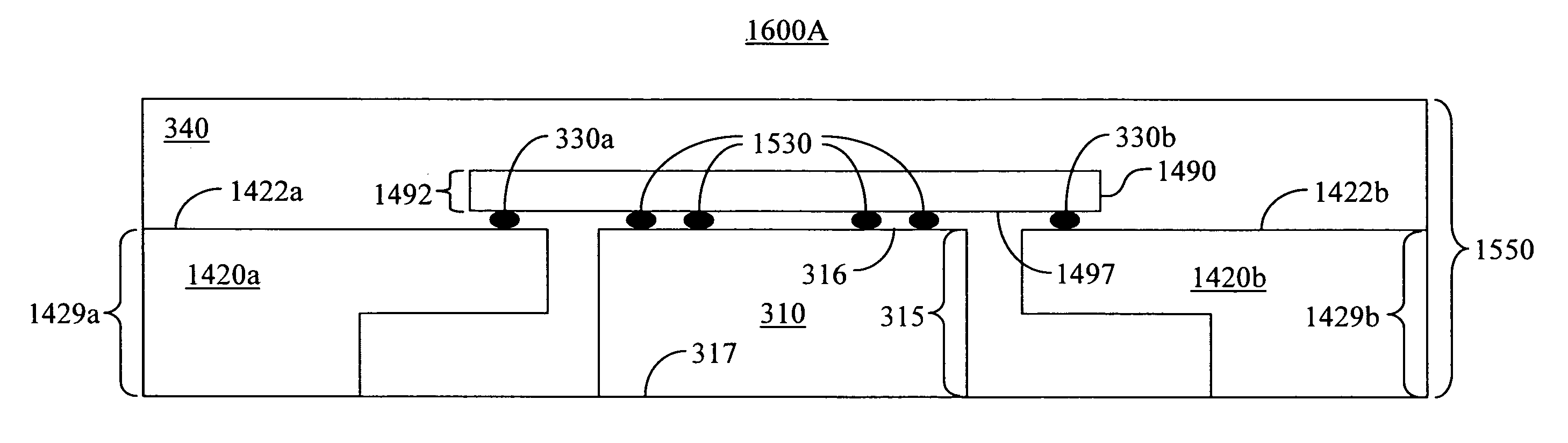
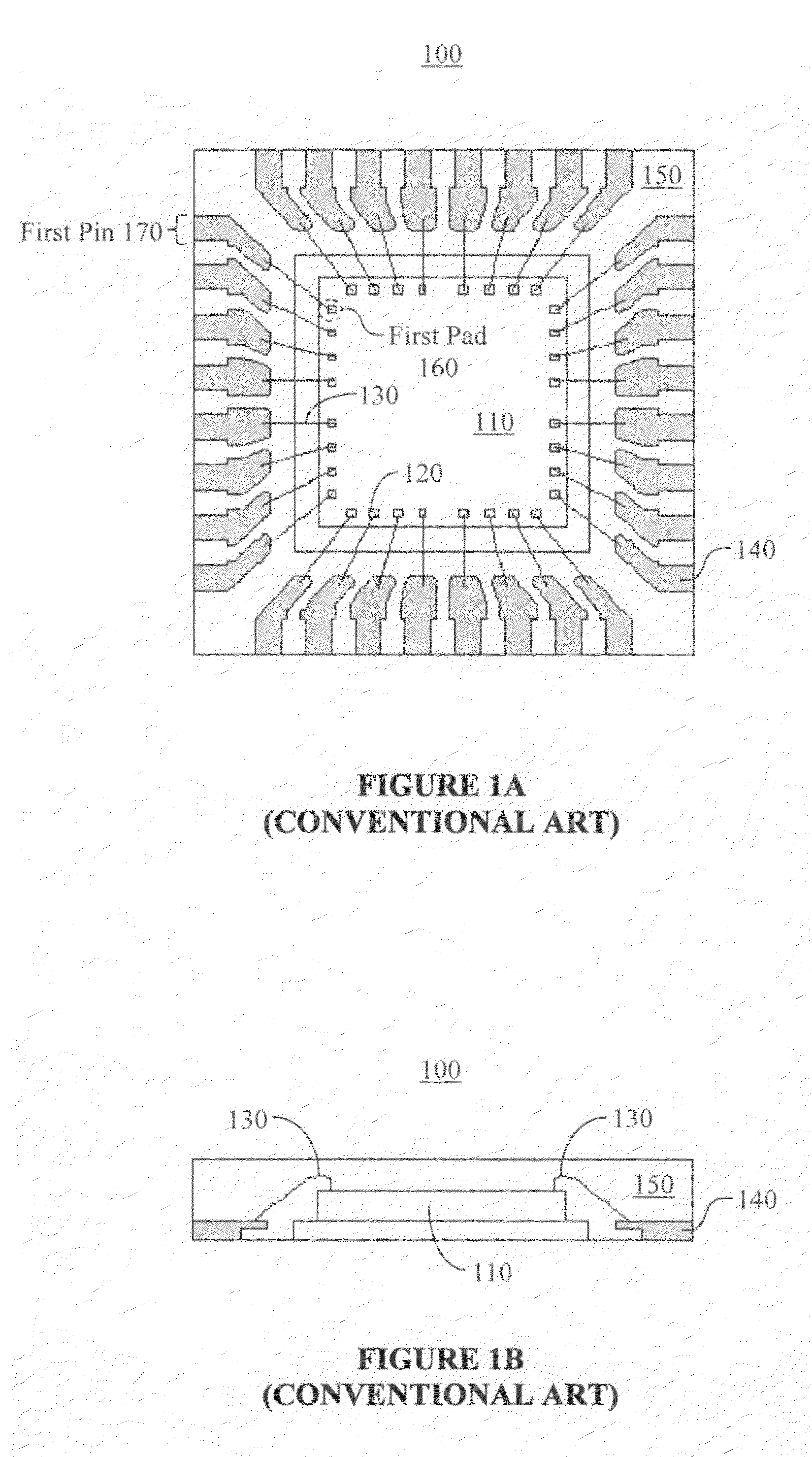
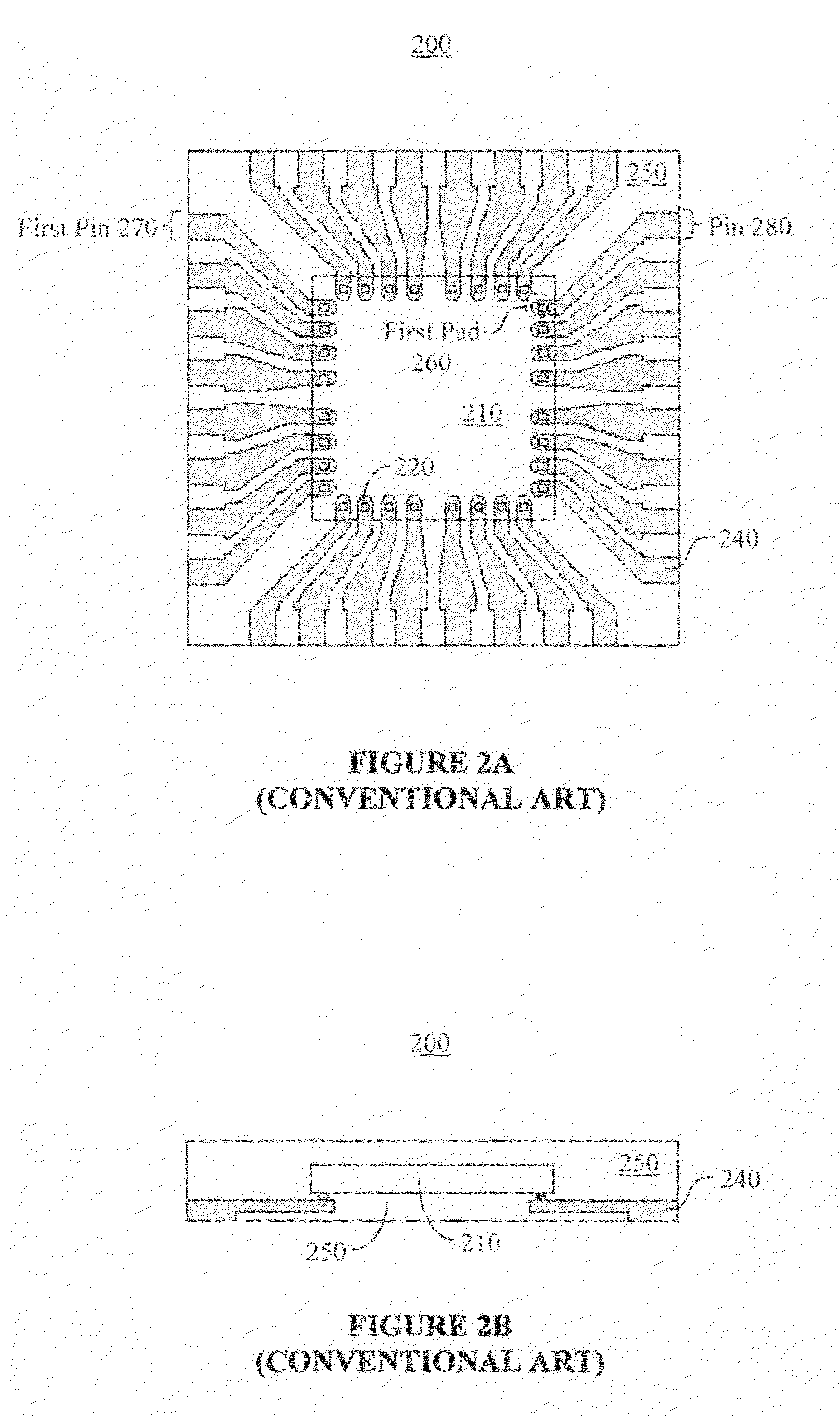
[0041]Reference will now be made in detail to embodiments of the present invention, examples of which are illustrated in the accompanying drawings. While the present invention will be discussed in conjunction with the following embodiments, it will be understood that they are not intended to limit the present invention to these embodiments alone. On the contrary, the present invention is intended to cover alternatives, modifications, and equivalents which may be included with the spirit and scope of the present invention as defined by the appended claims. Furthermore, in the following detailed description of the present invention, numerous specific details are set forth in order to provide a thorough understanding of the present invention. However, embodiments of the present invention may be practiced without these specific details. In other instances, well-known methods, procedures, components, and circuits have not been described in detail so as not to unnecessarily obscure aspect...


PUM


Abstract

A semiconductor device package, a method of fabricating a semiconductor device package and a method of testing an integrated circuit utilizing a semiconductor device package are disclosed. Embodiments create a flip-flop semiconductor device package by coupling a semiconductor device, with a wire-bonded arrangement of conductive pads, in a face-up orientation beneath etched portions of multiple leadfingers. The flip-flop package offers improved signaling properties, durability, reliability, and package density at reduced cost given that the conductive pads of the device couple directly to the leadfingers, without requiring the manufacture of a new device or the rerouting of signal paths. The height of the package is also reduced by utilizing space beneath the etched portions of the leadfingers that was unused in conventional solutions. Additionally, the flip-flop configuration provides convenient means for exposing surfaces of the device and/or surfaces of the leadfingers.

Description

RELATED APPLICATIONS[0001]The present application is related to U.S. patent application Ser. No. 11 / 731,056, filed Mar. 30, 2007, entitled “FLIP-FLOP SEMICONDUCTOR DEVICE PACKAGING USING BENT LEADFINGERS,” naming Carlo Gamboa as the inventor, assigned to the assignee of the present invention. That application is incorporated herein by reference in its entirety and for all purposes.[0002]The present application is related to U.S. patent application Ser. No. 11 / 731,088, filed Mar. 30, 2007, entitled “FLIP-FLOP SEMICONDUCTOR DEVICE PACKAGING USING AN INTERPOSER,” naming Bo Chang as the inventor, assigned to the assignee of the present invention. That application is incorporated herein by reference in its entirety and for all purposes.BACKGROUND OF THE INVENTION[0003]As technology evolves, more and more applications demand integrated circuits with higher performance and smaller size. For example, many circuits utilize higher signaling speeds requiring integrated circuits with improved s...

Claims


Application Information

Patent Timeline
Patent Type & Authority Patents(United States)
IPC IPC(8): H01L21/44
CPCH01L23/3107H01L23/49531H01L23/49548H01L23/49551H01L23/49572H01L2224/48247H01L2224/16245H01L2224/49171H01L2924/3011H01L24/48H01L24/49H01L2924/30107H01L2224/48465H01L2924/00H01L2224/05554H01L2224/48091H01L2924/00014H01L2924/14H01L2924/181H01L2924/18161H01L2924/00012H01L2224/45099H01L2224/45015H01L2924/207
Inventor CHANG, BO SOON
Owner MONTEREY RES LLC
Why Eureka
Try Eureka