Gate driver circuit for H bridge circuit

a gate driver and circuit technology, applied in the field of h bridge circuits, can solve problems such as increase the power dissipation, potential problems such as malfunction errors and performance degradation of circuits, and other problems

Active Publication Date: 2011-05-10
NXP USA INC
View PDF17 Cites 9 Cited by
  • Summary
  • Abstract
  • Description
  • Claims
  • Application Information

AI Technical Summary

Benefits of technology

The increase of gate voltage can increase the current in the NMOS device 12, which can greatly decrease the current in the body diode and the parasitic NPN device due to current conservation. The decrease of the parasitic NPN current can significantly reduce power dissipation and the injection of minority carriers, which will induce both a function error and performance degradation of the H bridge circuit. Further, the present invention can prevent large current punch-through between the PMOS device 11 and the NMOS device 12 because the NMOS device 12 will work in the sub-threshold region during the punch through time.
During dead time, the gate voltage of the NMOS device is biased at 0.1˜0.4V to overcome the problems of minority carrier injection and power dissipation as compared with VG=0 in a conventional H bridge circuit. The increase of gate voltage can increase the current in the NMOS device which can greatly decrease the current in the body diode and the parasitic NPN device due to current conservation. The decrease of the parasitic NPN current can significantly reduce power dissipation and the injection of minority carriers, which will induce both a function error and performance degradation of the H bridge circuit. Further, the present invention can prevent large current punch-through between the PMOS device and the NMOS device because the NMOS device will work in a sub-threshold region during the punch through time.
The present invention can be used in an H bridge circuit product without a Schottky diode and a Buck converter product without a Schottky diode.

Problems solved by technology

Injection of a substrate minority carrier can induce a function error and performance degradation of the circuit.
The large current in the parasitic NPN device can sometimes greatly increase the power dissipation and other potential issues, such as self-heating effects, reliability, and so on.

Method used


Image

  • Gate driver circuit for H bridge circuit
  • Gate driver circuit for H bridge circuit
  • Gate driver circuit for H bridge circuit

Examples


first embodiment

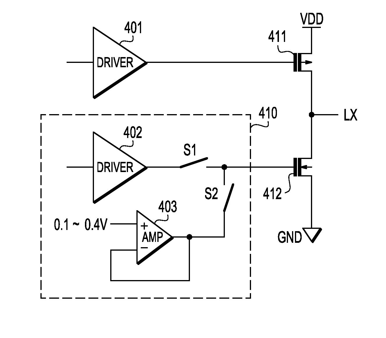
As shown in FIG. 4A, in the present invention, both the inverting input and the output of the AMP 403 are coupled to the gate of the first NMOS device 412 via the second switch S2.

FIG. 4B is a schematic diagram showing a gate driver circuit according to a second embodiment of the present invention. As shown in FIG. 4B, the H bridge circuit according to the second embodiment of the present invention comprises a first PMOS device 411 and a first NMOS device 412. The first PMOS device 411 and the first NMOS device 412 are coupled in series between a voltage source VDD and a ground GND. A voltage output from a connection point of the first PMOS device 411 and the first NMOS device 412 is provided to a load LX. The first PMOS device 411 is coupled to the voltage source VDD, and the first NMOS device 412 is coupled to the ground GND. A gate driver 401 for the first PMOS device 411 is coupled to a gate of the first PMOS device 411, and a gate driver circuit 420 for the first NMOS device 41...

second embodiment

The driver circuit of FIG. 4B differs from the driver circuit of FIG. 4A in that in the present invention, the driver comprises two pre-drivers 402a and 402b, the first switch S1 comprises two first switches S1, and the second switch S2 comprises two second switches S2. The gate driver circuit 420 for the first NMOS device 412 further comprises a second PMOS device 421 and a second NMOS device 422 that are coupled with each other in series between the voltage source and the GND. A voltage output from a connection point of the second PMOS device 421 and the second NMOS device 422 is provided to the gate of the first NMOS device 412. The second PMOS device 421 is coupled to the voltage source, and the second NMOS device 422 is coupled to the GND. The outputs of the two pre-drivers 402a and 402b are coupled to a gate of the second PMOS device 421 and a gate of the second NMOS device 422, respectively, via the two first switches S1. The output of the AMP 403 is coupled to the gate of th...


PUM


Abstract

An H bridge circuit includes a gate driver circuit coupled to a gate of an NMOS device. The output of the gate driver circuit is at a voltage from 0.1V to 0.4V during a dead time of the H bridge circuit. The gate voltage of the NMOS device is biased at 0.1˜0.4V to overcome the problems of minority carrier injection and power dissipation as compared with VG=0 in a conventional H bridge circuit.

Description

BACKGROUND OF THE INVENTIONThe present invention relates to an H bridge circuit, and more particularly, to a new gate drive method for an H bridge circuit.An H bridge circuit is a type of circuit that is well known to those the skilled in the art. If there is no Schottky diode in the H bridge circuit, the current through the inductor can induce the turn-on of both the body diode and the parasitic NPN device during dead time.FIG. 1 is a schematic diagram showing a cross-section of a conventional isolated NMOS device. The minority carrier injection and power dissipation will happen when there is a large current in the parasitic NPN device.In the prior art, the gate drive voltage is 0 and there is no current assignment between the NMOS device and the parasitic NPN device during the dead time. Injection of a substrate minority carrier can induce a function error and performance degradation of the circuit. The large current in the parasitic NPN device can sometimes greatly increase the p...

Claims


Application Information

Patent Timeline
Patent Type & Authority Patents(United States)
IPC IPC(8): H03K3/00
CPCH03K17/08122H02M7/538
Inventor ZHENG, IVENLI, WALEYWEI, LINPENGZHAO, HONGWEILI, WEIYING
Owner NXP USA INC
Why Eureka
Try Eureka