Electronic device for the transport of numerical information

a numerical information and electronic device technology, applied in the field of electronic devices, can solve the problems of mw and at greater cost, inability to operate below a differential voltage swing of 700 mw, and high power consumption, and achieve the effects of small resistance area, increased bit transmission rate, and high magnetoresistan

Inactive Publication Date: 2011-05-17
CENT NAT DE LA RECH SCI 15
View PDF8 Cites 27 Cited by
  • Summary
  • Abstract
  • Description
  • Claims
  • Application Information

AI Technical Summary

Benefits of technology

[0024]Usually, the easy-magnetization axis of the soft layer of each magnetoresistive stack is aligned with the magnetization of the hard layer: Thus, reversal of the magnetization of the hard layer between two stable positions (at 0 and 180 degrees relative to the easy-magnetization axis) makes it possible to obtain magnetic states which are parallel and anti-parallel to the magnetization of the hard layer, thereby maximizing the variations in resistance.
[0072]In one advantageous embodiment of the invention, the magnetic junctions may have a small resistance area and a high magnetoresistance, preferably in excess of 200%. This increases the bit transmission rate because the magnetic conversion rate is in excess of the velocity of electricity (CMOS).

Problems solved by technology

As for the ECL and CML standards, these make it possible to transport information at higher bit rates, typically of the order of 2 Gb / s but with a power consumption which is markedly higher than that in the case of the LVDS standard, typically of the order of 200 mW and at greater cost because these standards use non-standard technology.
Consequently, the dynamic power required to generate the signals which transport the digital information is of the order of 2.1 mW, and cannot operate below a differential voltage swing of 700 mW.
In addition, bearing in mind the electrical impedance of the transmission line, the integrity of the transmitted signals cannot be guaranteed where transmission distances exceed 15 m. Moreover, this impedance prevents these electronic devices from addressing digital information from a single transmitter to a plurality of receivers because the signals are degraded when they are received.

Method used


Image

  • Electronic device for the transport of numerical information
  • Electronic device for the transport of numerical information
  • Electronic device for the transport of numerical information

Examples


Embodiment Construction

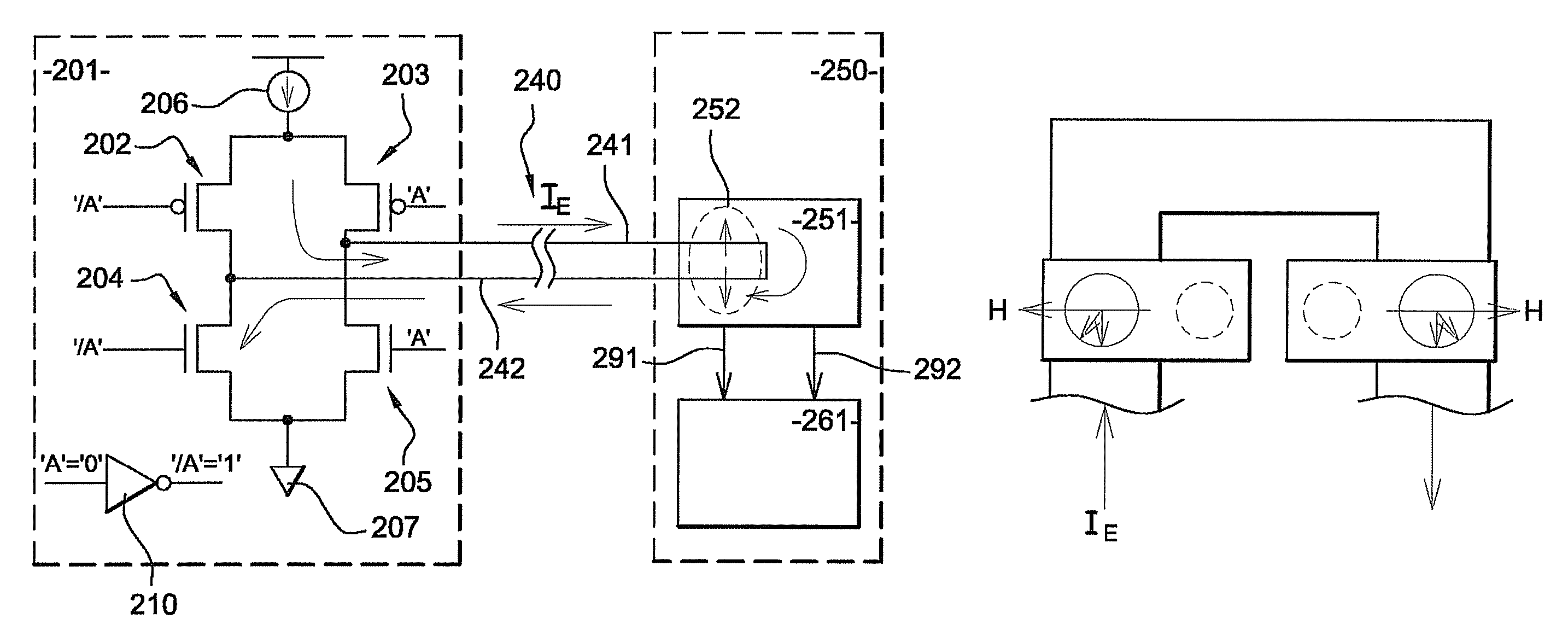
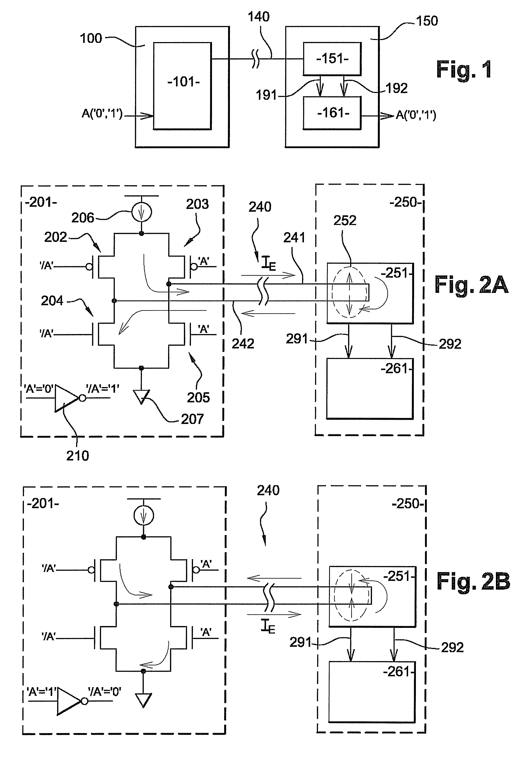
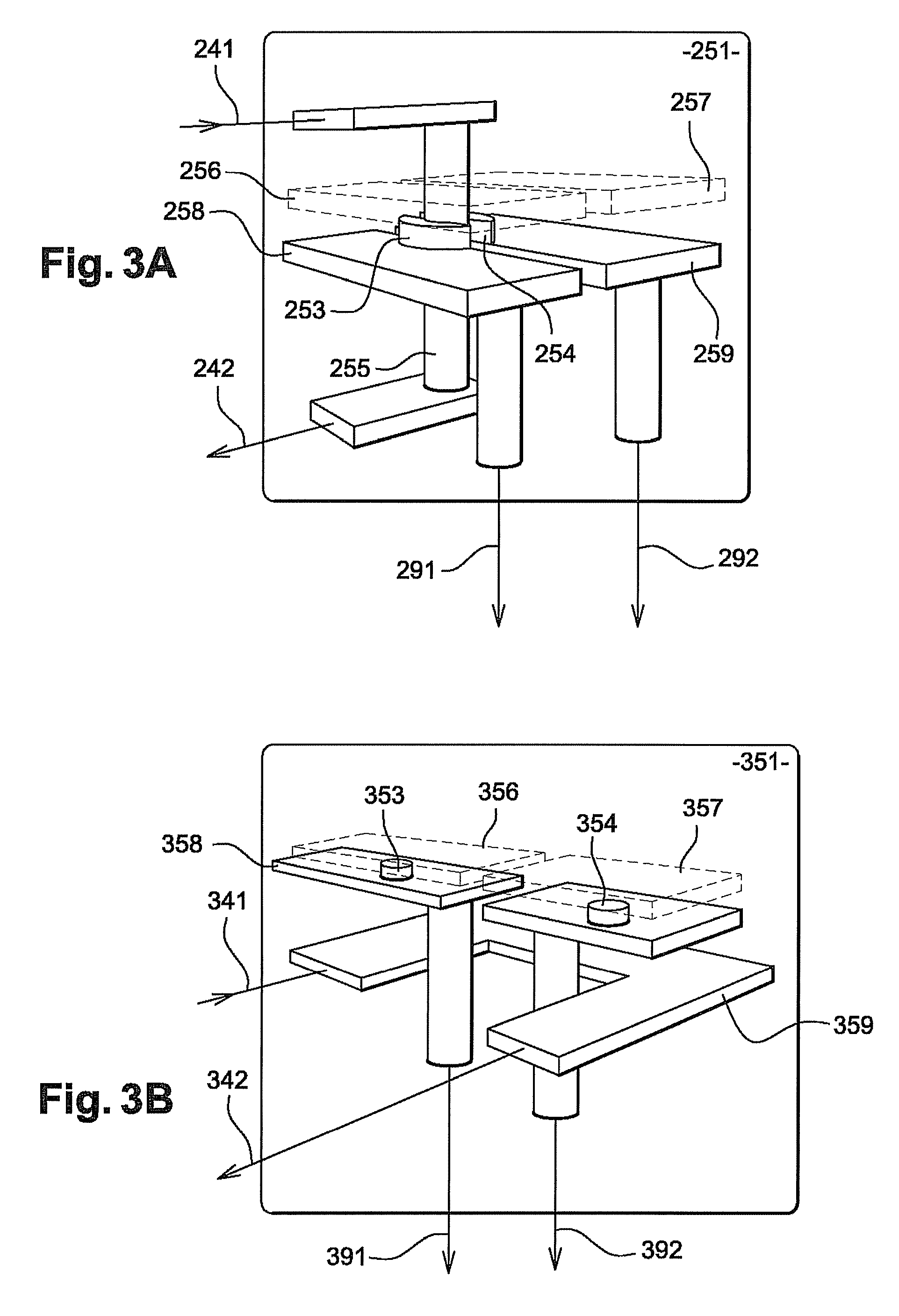
[0080]FIG. 1 shows the units which make up an electronic device in accordance with the invention. A transmitter 100 comprising an integrated circuit 101 is designed to write to the first stage 151 of a receiver 150 via a write loop 140. The term “write” actually denotes the output of electrical signals by current modulation from integrated write circuit 101 to the first stage 151 of receiver 150. Receiver 150 also comprises an integrated read circuit 161 which is electrically connected to first stage 151 via connections 191 and 192.

[0081]The length of write loop or line 140 represents the distance over which the “0” and “1” digital signals are transported. Obviously, the digital information (signals) reach integrated write circuit 101 from a source situated upstream and shown schematically in FIG. 1. Similarly, integrated read circuit 161 of receiver 150 transmits digital information originating from magnetoresistive stage 151 which it has decoded to one or more other components cap...


PUM


Abstract

An electronic device designed to transport digital information (“0”, “1”) over long distances, including a transmitter generating current pulses and at least one assembly of receivers converting the received current pulses into logic pulses which are compatible with the operation of standard electronic logic circuits. Each receiver includes a pair of magnetoresistive stacks containing at least one hard ferromagnetic layer and one soft ferromagnetic layer separated by a non-ferromagnetic interlayer, the hard layer of each of the magnetoresistive stacks being pinned in a magnetic orientation perpendicular to an easy-magnetization axis which is used as a reference for the soft layer of the same stack. The soft layer of each magnetoresistive stack has a magnetic orientation which can be modulated by the magnetic field generated by current pulses delivered by the transmitter so as to cause modification of the transverse resistance of the stack sufficient to trigger an electrical signal.

Description

FIELD OF THE INVENTION[0001]The present invention relates to an electronic device for transporting digital information over long distances comprising a transmitter associated with a magnetoresistive receiver. The term “digital information” is taken to mean “0s” and “1s” which are also referred to as logic information or signals as opposed to analogue signals.[0002]The present invention therefore relates to the field of IT infrastructure designed for high-speed transmission of data between adjacent or distant components by means of wire connections or lines.[0003]The term “adjacent components” denotes components which are part of a single board whereas the term “distant components” denotes, for example, two peripherals which are more or less far apart such as the graphics card and the monitor of a microcomputer.BACKGROUND OF THE INVENTION[0004]In the field of microelectronics, processors are currently being fabricated with increasingly higher clock frequencies, ranging typically from...

Claims


Application Information

Patent Timeline
Patent Type & Authority Patents(United States)
IPC IPC(8): H03K17/16H03K19/003
CPCH01L27/101H04L25/0266H04L25/0272
Inventor JAVERLIAC, VIRGILE
Owner CENT NAT DE LA RECH SCI 15
Why Eureka
Try Eureka