Method for manufacturing thin film transistor and display device
a technology of thin film transistor and display device, which is applied in the direction of conductive pattern formation, semiconductor/solid-state device details, instruments, etc., can solve the problem of increasing manufacturing cost, reducing the number of processes, and affecting the appearance of large substrates having a side of 1 meter or more, so as to reduce costs, reduce manufacturing costs, and reduce material loss
- Summary
- Abstract
- Description
- Claims
- Application Information
AI Technical Summary
Benefits of technology
Problems solved by technology
Method used
Image
Examples
embodiment 1
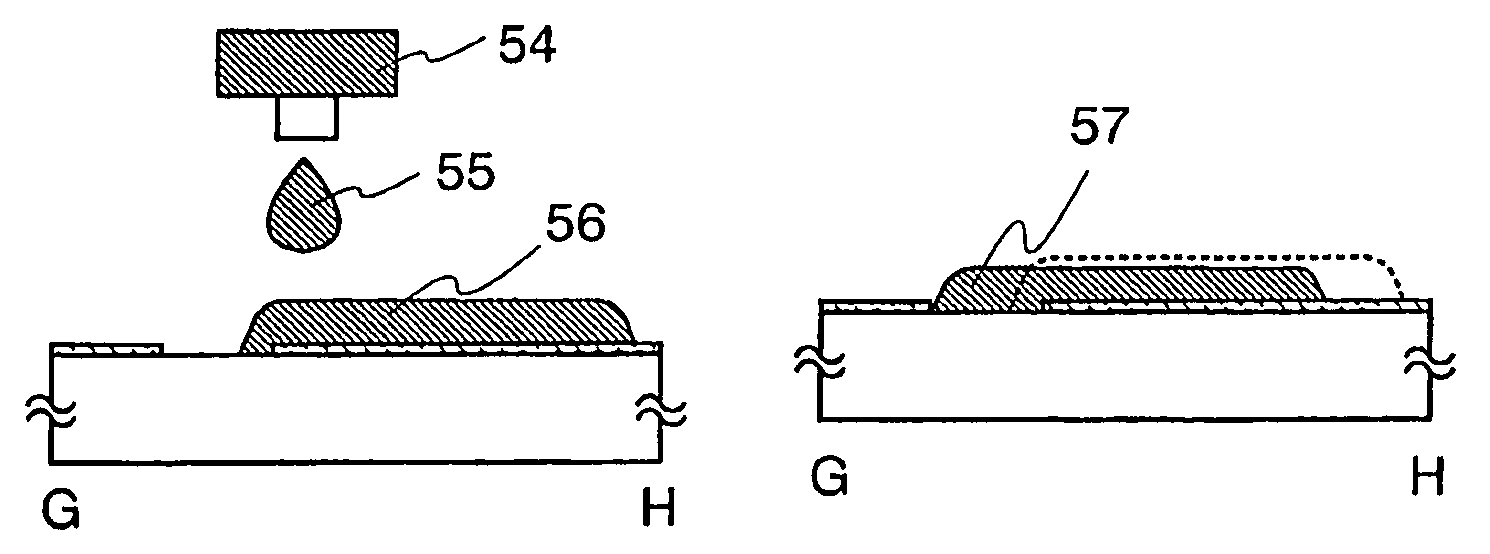
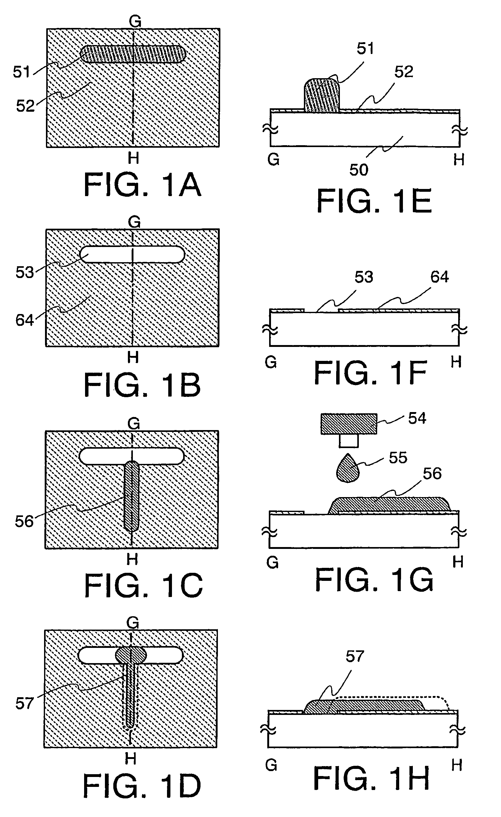
[0069]Although the present invention will be fully described by way of embodiments with reference to the accompanying drawings, it is to be understood that various changes and modifications will be apparent to those skilled in the art. Therefore, unless otherwise such changes and modifications depart from the scope of the present invention hereinafter described, they should be construed as being included therein. Through the drawing of the embodiments, same components are denoted by same numerals, and will not be further explained.
[0070]FIG. 29A illustrates a top view for showing an example of a structure of a display panel according to the present invention. A pixel portion 2701 composed of pixels 2702 in a matrix configuration over a substrate 2700 having an insulating surface, a scanning line side input terminal 2703, and a signal line side input terminal 2704 are formed. The number of pixels may be set according to various specifications, for example, 1024×768×3 (RGB) for XGA, 1...
embodiment 2
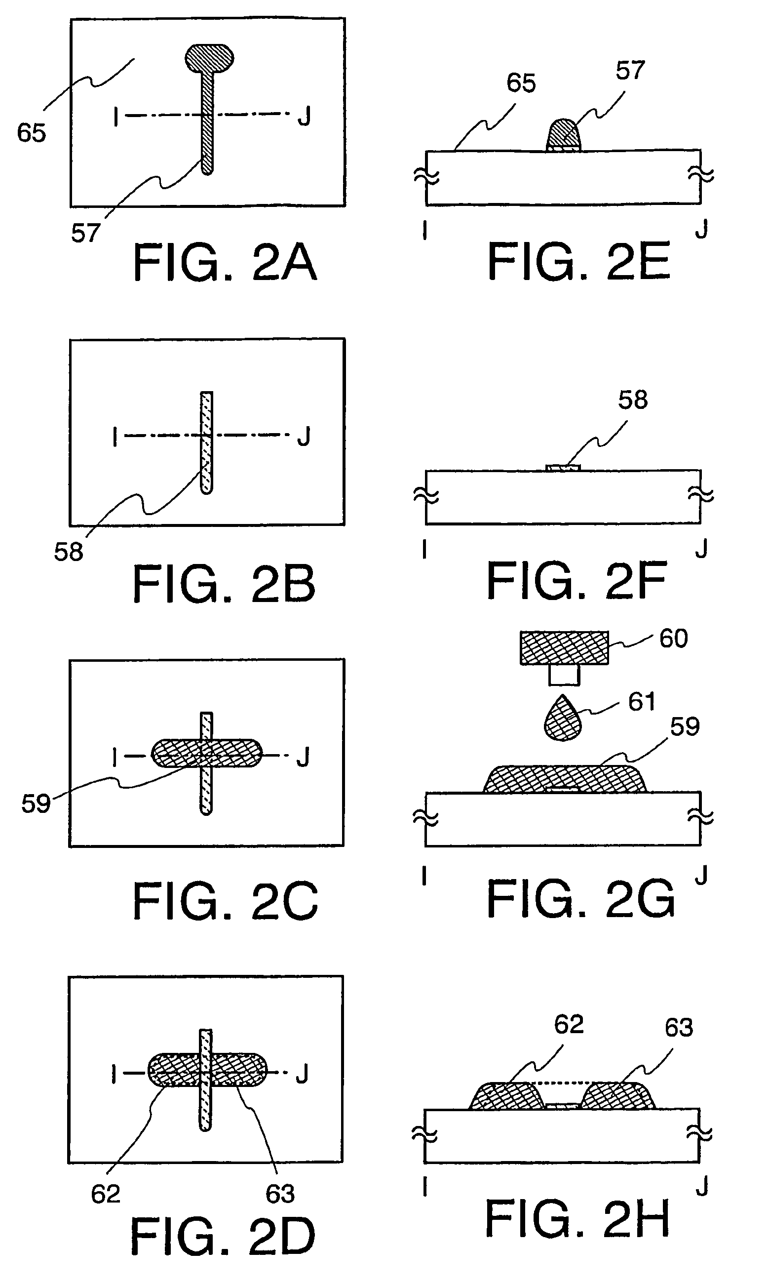
[0102]An embodiment of the present invention is explained with reference to FIGS. 2A to 2H. FIGS. 2A to 2D are top views of a pattern. FIGS. 2E to 2H are cross-sectional views taken along line I-J of FIGS. 2A to 2D. FIG. 2A to 2D correspond respectively to FIGS. 2E to 2H.
[0103]In this embodiment, another example of forming a pattern according to the present invention is explained. In Embodiment 1, an example of forming a pattern into a fine line is explained. In this embodiment, an example of forming finely spaced apart patterns with good controllability is explained.
[0104]FIG. 2A illustrates the state that a low wettability substance 52 that has an effect of imparting low wettability is removed from the state illustrated in FIG. 1D using a pattern 57 as a mask. As illustrated in FIG. 2E, only the low wettability substance 52 is left below the pattern 57 and the periphery thereof is a high wettability region 65. The high wettability region has high wettability since it has not the l...
embodiment 3
[0107]This embodiment is explained with reference to FIGS. 38A to 38D. FIGS. 38A to 38D illustrates a top view of a pattern.
[0108]This embodiment shows an example of forming a pattern formed to be a fine line in Embodiment 1 is formed further longer to form a fine and long pattern.
[0109]A plurality of masks 71a, 71b, and 71c are provided spaced apart over a substrate 70. Thereafter, a low wettability substance 72 is formed by using the masks 71a, 71b, and 71c (FIG. 38A). Then, the masks 71a, 71b, and 71c are removed by etching. A low wettability region 78, and high wettability regions 73a, 73b, and 73c are selectively formed over the substrate 70 (FIG. 38B).
[0110]A droplet of a composition containing a pattern formation material having fluidity is discharged so as to be crossed the high wettability regions 73a, 73b, and 73c and to be straddled the low wettability region by droplet discharging. The composition containing a pattern formation material is discharged from a nozzle as a d...
PUM
| Property | Measurement | Unit |
|---|---|---|
| contact angle | aaaaa | aaaaa |
| grain diameters | aaaaa | aaaaa |
| contact angle | aaaaa | aaaaa |
Abstract
Description
Claims
Application Information
 - R&D
- Intellectual Property
- Life Sciences
- Materials
- Tech Scout
- Unparalleled Data Quality
- Higher Quality Content
- 60% Fewer Hallucinations
Browse by: Latest US Patents, China's latest patents, Technical Efficacy Thesaurus, Application Domain, Technology Topic, Popular Technical Reports.
© 2025 PatSnap. All rights reserved.Legal|Privacy policy|Modern Slavery Act Transparency Statement|Sitemap|About US| Contact US: help@patsnap.com


