

Silicon interposer-based hybrid voltage regulator system for VLSI devices
- Summary
- Abstract
- Description
- Claims
- Application Information
AI Technical Summary
Problems solved by technology
Method used
Image

Examples
Embodiment Construction
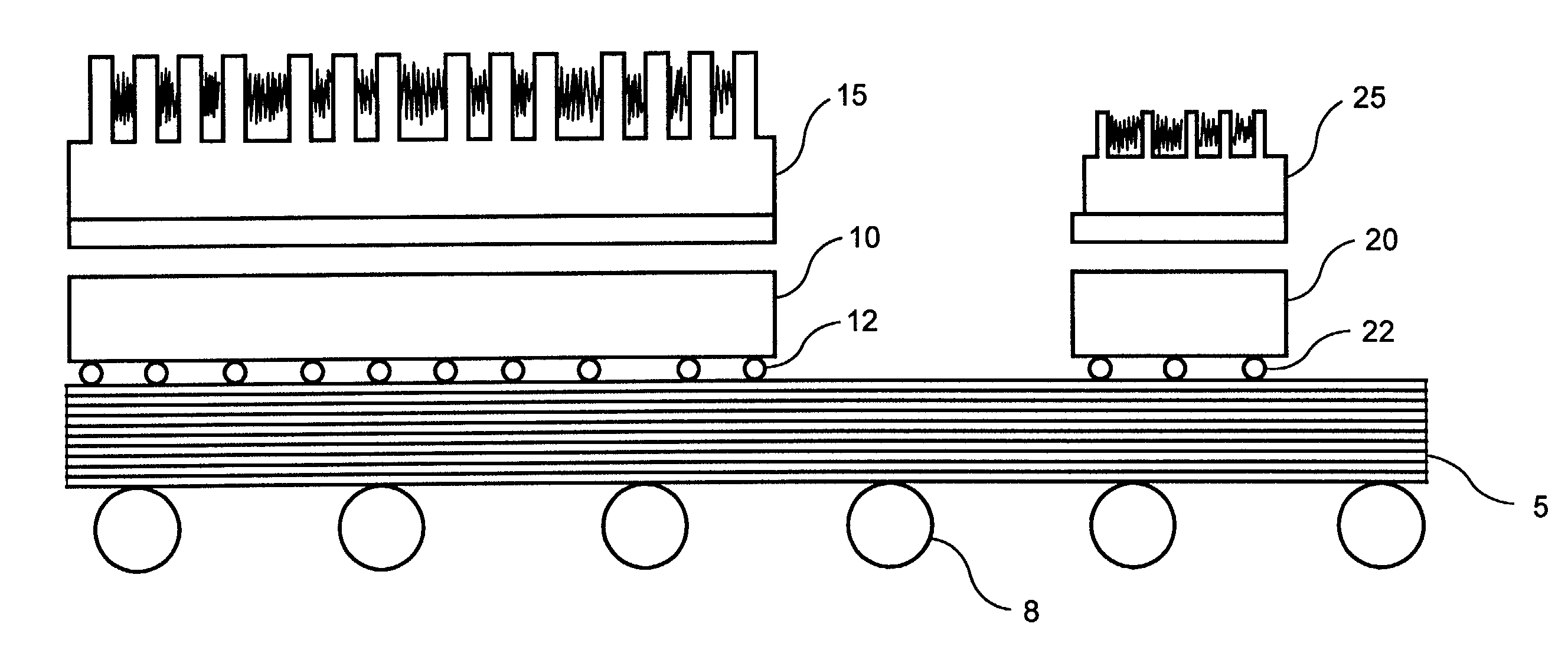
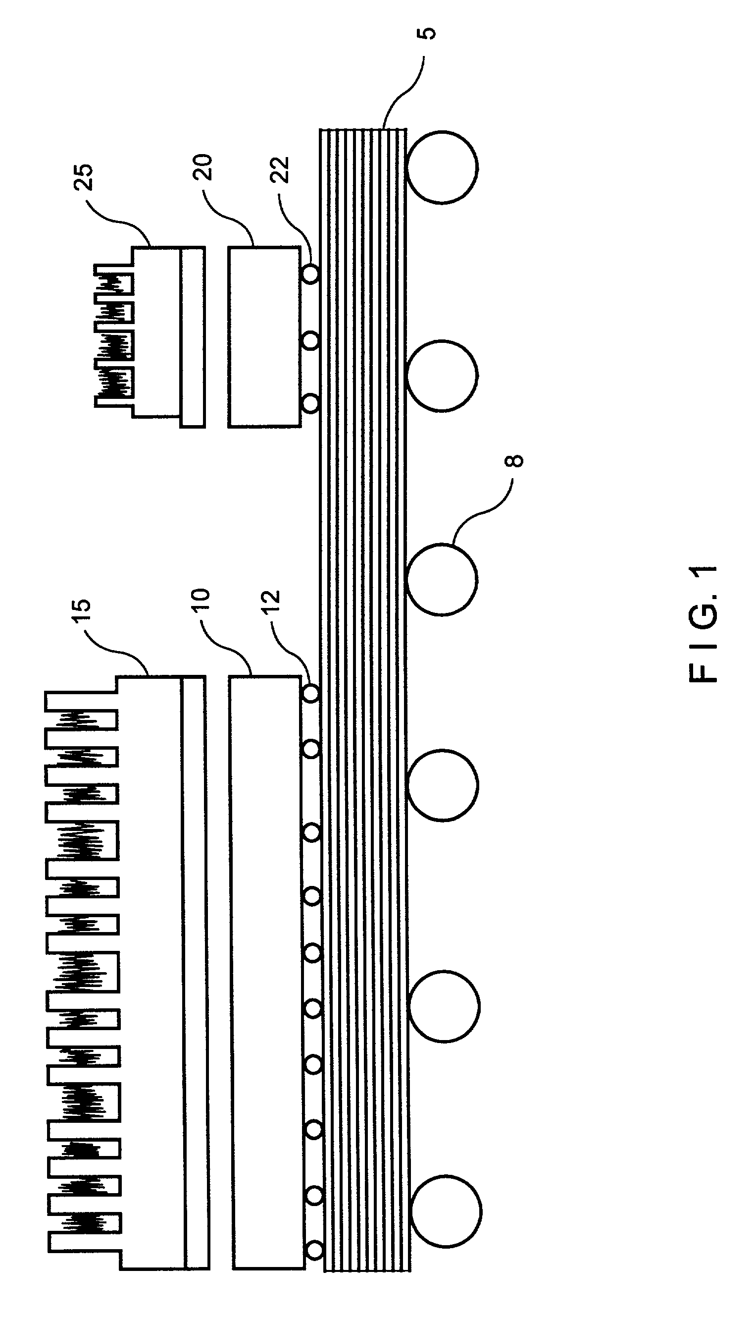
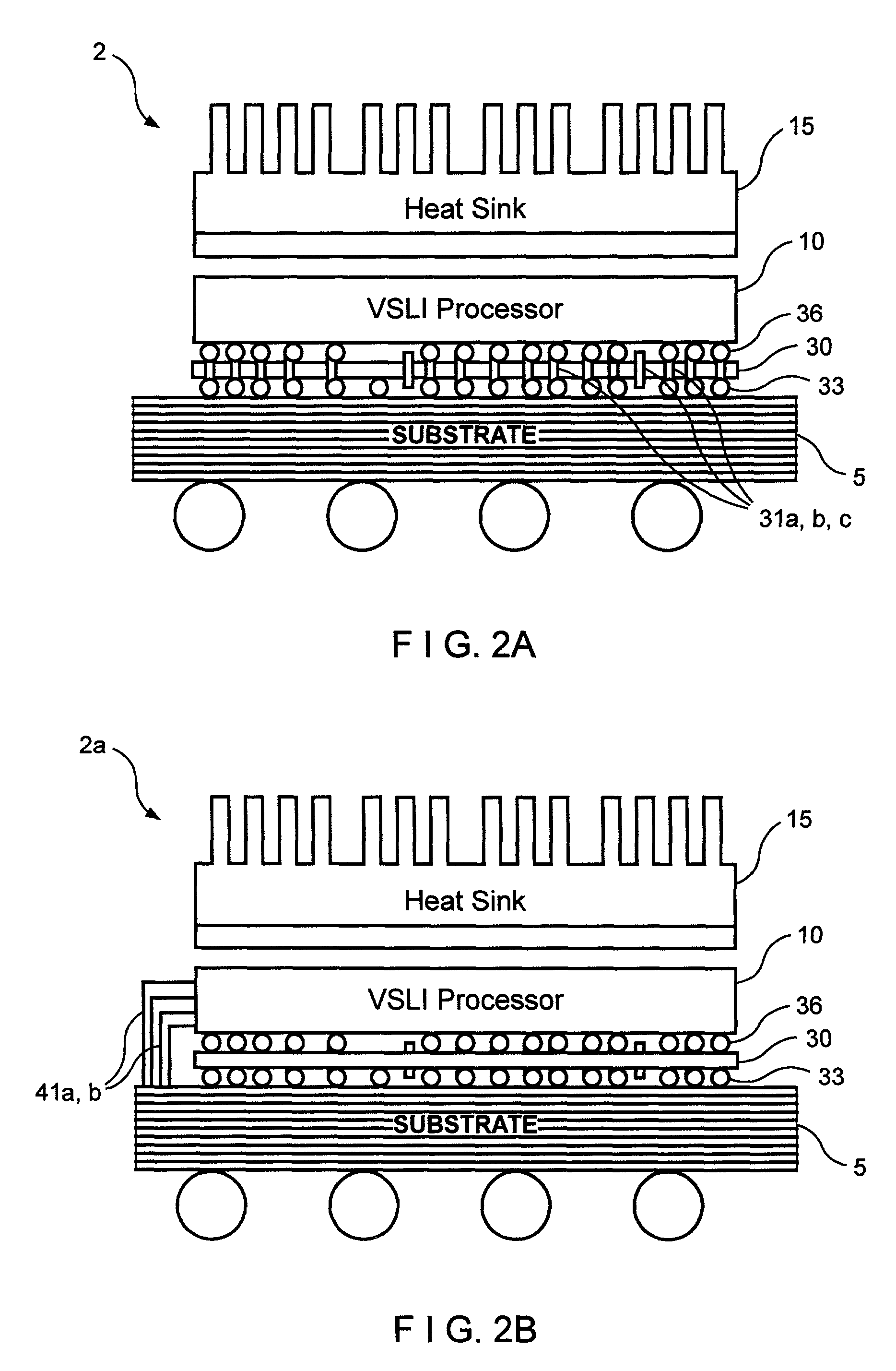
[0010]In accordance with the present invention, a stacked-die approach is used for integrating voltage regulator modules with VLSI chips to minimize IR voltage drops in high current delivery pathways at low voltages. In the stacked-die approach a silicon interposer layer is stacked so that it adjoins and faces a VLSI circuit or processer die. The two-dimensional interface and minimal separation distance between the interposer layer and the VLSI die helps ensure minimal IR voltage drops and eliminates supply bottlenecks. Within the interposer layer, a hybrid voltage regulator array arrangement assists in the minimization of on-die voltage droops in high di / dt events. The array includes relatively fast, high-bandwidth linear regulators and relatively slower, but more efficient low-bandwidth switching regulators. By positioning linear regulators in so-called ‘hot spots’ on the VLSI die that intermittently demand high current levels, rapid adjustments in voltage supply levels can be ach...
PUM
 Abstract
Description
Claims
Application Information