String interconnection and fabrication of inverted metamorphic multijunction solar cells

a solar cell and string interconnection technology, applied in the field of string interconnection and fabrication of inverted metamorphic multijunction solar cells, can solve the problems of presenting a number of practical difficulties and tending to be more complex in manufactur

Active Publication Date: 2011-06-14
SOLAERO TECH CORP
View PDF104 Cites 40 Cited by
  • Summary
  • Abstract
  • Description
  • Claims
  • Application Information

AI Technical Summary

Problems solved by technology

Compared to silicon, III-V compound semiconductor multijunction devices have greater energy conversion efficiencies and generally more radiation resistance, although they tend to be more complex to manufacture.
However, the materials and structures for a number of different layers of the cell proposed and described in such reference present a number of practical difficulties, particularly relating to the most appropriate choice of materials and fabrication steps.

Method used


Image

  • String interconnection and fabrication of inverted metamorphic multijunction solar cells
  • String interconnection and fabrication of inverted metamorphic multijunction solar cells
  • String interconnection and fabrication of inverted metamorphic multijunction solar cells

Examples


second embodiment

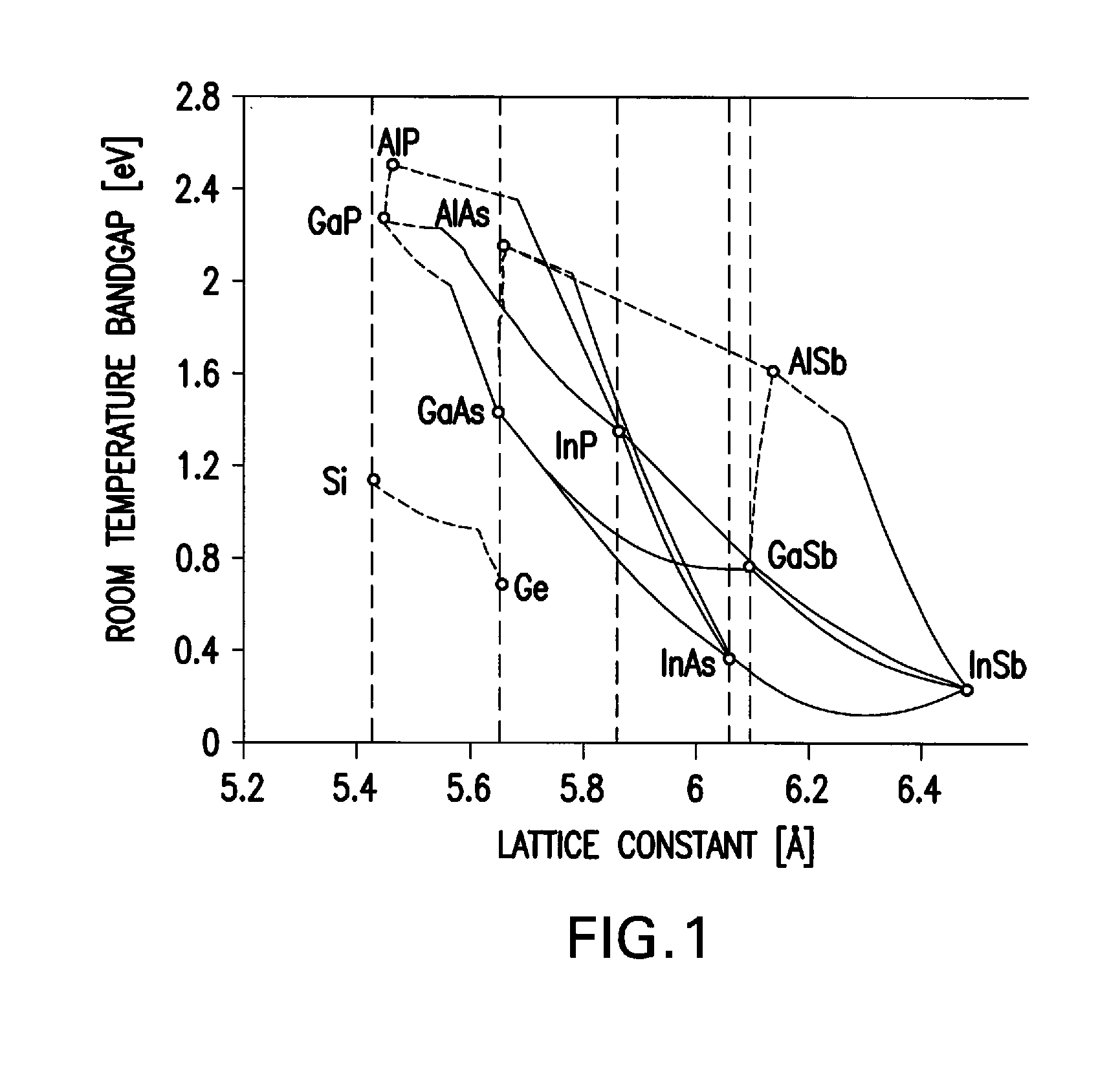
[0100]Although one embodiment of the present invention utilizes a plurality of layers of InGaAlAs for the metamorphic layer 116 for reasons of manufacturability and radiation transparency, other embodiments of the present invention may utilize different material systems to achieve a change in lattice constant from subcell B to subcell C. Thus, the system of Wanlass using compositionally graded InGaP is the present invention. Other embodiments of the present invention may utilize continuously graded, as opposed to step graded, materials. More generally, the graded interlayer may be composed of any of the As, P, N, Sb based III-V compound semiconductors subject to the constraints of having the in-plane lattice parameter greater or equal to that of the second solar cell and less than or equal to that of the third solar cell, and having a band gap energy greater than that of the second solar cell.

[0101]In another embodiment of the present invention, an optional second barrier layer 117 ...

third embodiment

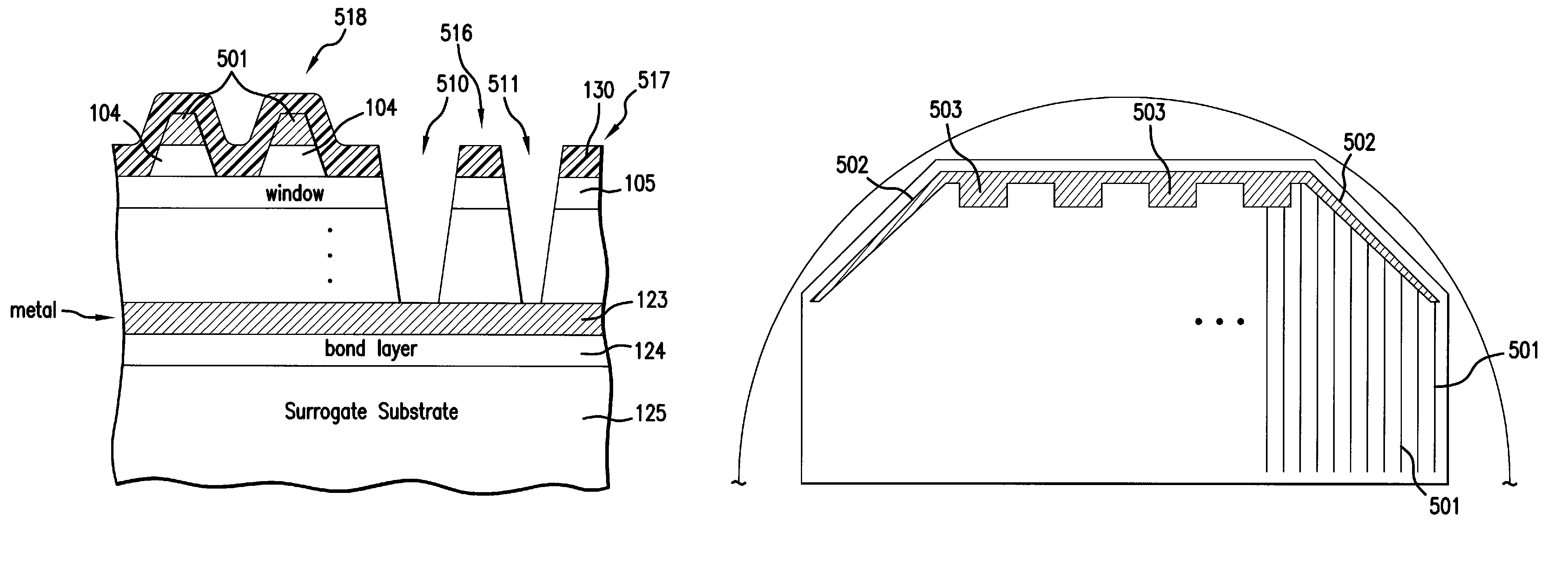
[0130]FIG. 14C is a cross-sectional view of the solar cell of FIG. 12B after the next process step in the present invention in which a cover glass 514 is secured to the top of the cell by an adhesive 513. The cover glass 514 is typically about 4 mils thick and preferably covers the entire channel 510, extends over a portion of the mesa 516, but does not extend to channel 511. Although the use of a cover glass is desirable for many environmental conditions and applications, it is not necessary for all implementations, and additional layers or structures may also be utilized for providing additional support or environmental protection to the solar cell.

[0131]FIG. 14D is a cross-sectional view of the solar cell of FIG. 14A after the next process step in some embodiments of the present invention in which the adhesive layer 124, the surrogate substrate 125 and the peripheral portion 517 of the wafer is entirely removed, leaving only the solar cell with the ARC layer 130 (or other layers ...


PUM


Abstract

A method of manufacturing a solar cell by providing a first substrate; depositing on a first substrate a sequence of layers of semiconductor material forming a solar cell including at least a top subcell and a bottom subcell; mounting a surrogate substrate on top of the sequence of layers adjacent to the bottom subcell; removing the first substrate to expose the surface of the top subcell; removing the surrogate substrate; and holding the solar cell on a vacuum chuck to support it for subsequent fabrication operations, such as attaching interconnects to the solar cells to form an interconnected array.

Description

GOVERNMENT RIGHTS STATEMENT[0001]This invention was made with government support under Contract No. FA9453-06-C-0345 awarded by the U.S. Air Force. The Government has certain rights in the invention.REFERENCE TO RELATED APPLICATIONS[0002]This application is related to co-pending U.S. patent application Ser. No. 12 / 362,213 and Ser. No. 12 / 362,225 filed simultaneously herewith.[0003]This application is related to co-pending U.S. patent application Ser. No. 12 / 337,014 and Ser. No. 12 / 337,043 filed Dec. 17, 2008.[0004]This application is related to co-pending U.S. patent application Ser. No. 12 / 271,127 and Ser. No. 12 / 271,192 filed Nov. 14, 2008.[0005]This application is related to co-pending U.S. patent application Ser. No. 12 / 267,812 filed Nov. 10, 2008.[0006]This application is related to co-pending U.S. patent application Ser. No. 12 / 258,190 filed Oct. 24, 2008.[0007]This application is related to co-pending U.S. patent application Ser. No. 12 / 253,051 filed Oct. 16, 2008.[0008]This ...

Claims


Application Information

Patent Timeline
Patent Type & Authority Patents(United States)
IPC IPC(8): H01L21/00
CPCH01L31/022425H01L31/03042H01L31/06875H01L31/1852H01L31/0693Y02P70/521Y02E10/544Y02P70/50
Inventor CORNFELD, ARTHURDIAZ, JACQUELINEVARGHESE, TANSEN
Owner SOLAERO TECH CORP
Why Eureka
Try Eureka