

Semiconductor device
a technology of semiconductors and devices, applied in the field of semiconductor devices, can solve the problems of difficult to ensure compatibility between the snm (static noise margin) and the write margin of the sram in a vth management width
- Summary
- Abstract
- Description
- Claims
- Application Information
AI Technical Summary
Benefits of technology
Problems solved by technology
Method used
Image

Examples
first embodiment
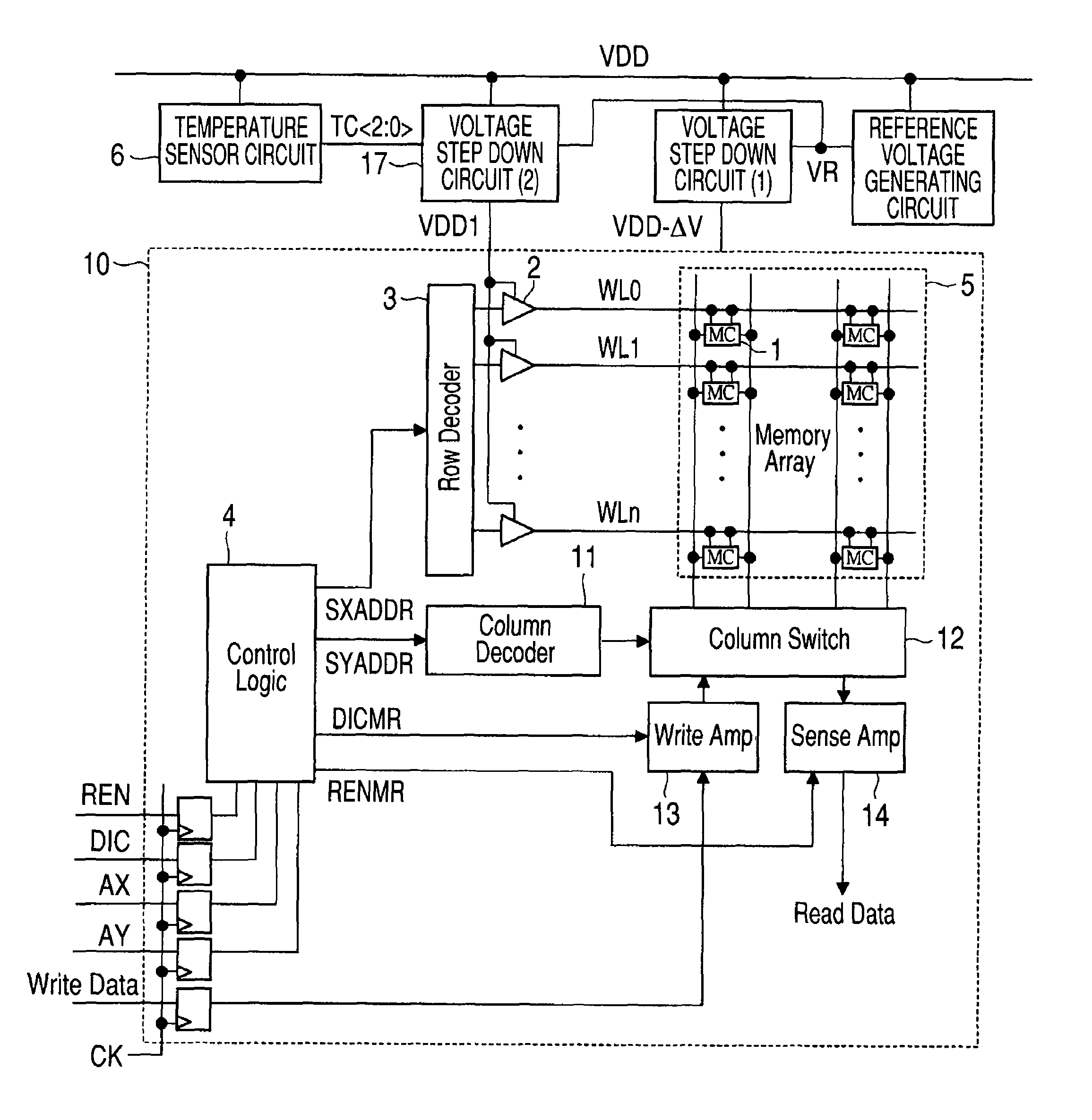
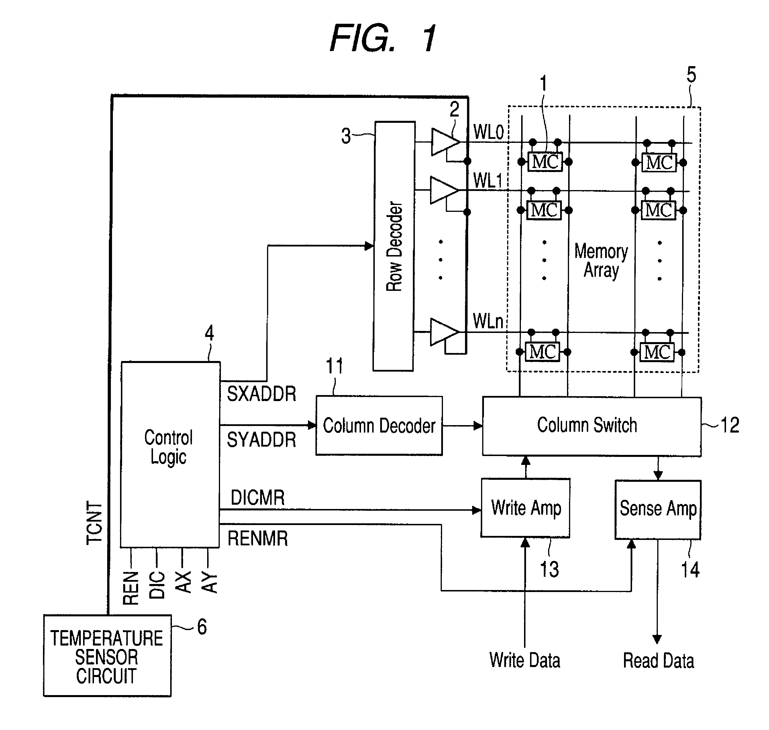
[0051]FIG. 1 is a block diagram showing a configuration example of an SRAM module in a semiconductor device according to the first embodiment of the invention.
[0052]First, one example of the configuration of the SRAM module in the semiconductor device according to the first embodiment will be described with reference to FIG. 1. The semiconductor device according to the first embodiment is formed over a single semiconductor substrate such as a silicon substrate, using a known semiconductor integrated circuit manufacturing technology, but is not limited thereto.
[0053]The SRAM module according to the first embodiment includes a memory cell array (Memory Array) 5 having a plurality of static memory cells (MCs) 1 arranged in a matrix, word drivers 2 for driving word lines WL0 to WLn coupled to the selection terminals of the memory cells 1, a row decoder (Row Decoder) 3, a control logic (Control Logic) 4 for controlling the write / read operation of the SRAM module, a column decoder (Column...
second embodiment
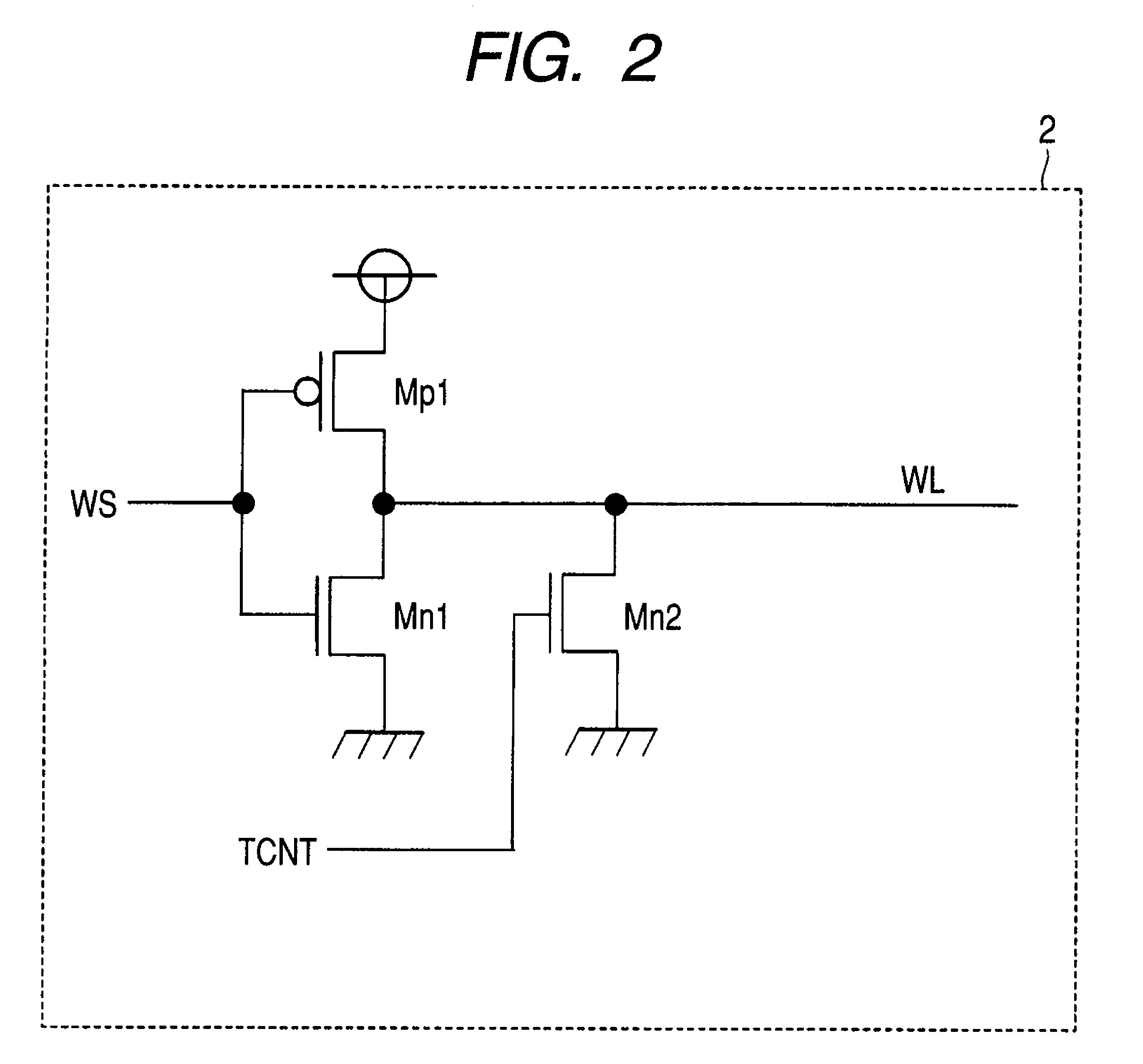
[0076]FIG. 9 is a block diagram showing a configuration example of an SRAM module in a semiconductor device according to the second embodiment of the invention. FIG. 10 is a circuit diagram showing a configuration example of the word driver 2 shown in FIG. 9.
[0077]In the second embodiment, in addition to the output of the temperature sensor circuit 6, a signal obtained by the cutting / non-cutting of a fuse (FUSE) 7 is inputted to the word drivers 2.
[0078]A signal TCNT is the output signal of the temperature sensor circuit 6, and a signal TCNT is the cut signal of the fuse 7. These signals TCNT and TCNT are sent to the word driver 2 and inputted to the respective gates of n-type MOS transistors Mn2 and Mn3 coupled to the word line WL. For example, during a wafer test, the threshold voltage Vth of an access MOS transistor (Access MOS) is evaluated in each chip by a monitor circuit provided inside the chip. If the threshold voltage Vth is lower than a reference value, the fuse 7 is cut ...
third embodiment
[0081]FIG. 11 is a block diagram showing a configuration example of an SRAM module in a semiconductor device according to the third embodiment of the invention. FIG. 12 is a circuit diagram showing a configuration example of the word driver 2 and a driver power supply circuit 8 shown in FIG. 11.
[0082]In the configuration example of FIG. 11, a signal TCNT is inputted to the driver power supply circuit 8, which supplies a power supply voltage VDDR to the word drivers 2. The voltage level of the power supply voltage VDDR outputted from the driver power supply circuit 8 is determined based on current pull by a p-type MOS transistor Mp1 and p-type MOS transistor Mp2 and Mp3 selected by the signal TCNT. Since the high level on the word line WL is the power supply voltage VDDR for the word drivers 2, the high level on the word line WL can be varied by the output of the temperature sensor circuit 6 and the cut signal of the fuse (FUSE) 7, as in the configuration example of FIG. 9 in the sec...
PUM
 Abstract
Description
Claims
Application Information