Design and fabrication methods of partial cladded write line to enhance write margin for magnetic random access memory

a random access memory and write line technology, applied in the field of mram design, can solve the problems of increasing the writing current proportionally, which is not desired for high density memory devices, and limiting the supply of available current, and the tendency of half-selected bits to be disturbed into the wrong sta

Active Publication Date: 2011-03-17
TAIWAN SEMICON MFG CO LTD
View PDF26 Cites 18 Cited by
  • Summary
  • Abstract
  • Description
  • Claims
  • Application Information

AI Technical Summary

Benefits of technology

[0015]One objective of the present invention is to provide a cladding design for a write or bit line proximate to a free layer in a MTJ that solves the half-select bit disturb problem without sacrificing the writing power of the write line or bit line to switch a magnetization direction in the free layer.

Problems solved by technology

One challenge associated with MRAM structures is not to disturb the so-called half selected bits under conductive lines (word line / bit line) that are not intended for programming.
However, this method will increase the writing current proportionally which is not desired for high density memory devices.
Another concern related to high density memory is that the transistor size limits the supply of available currents.
Unfortunately, the magnetic interaction between ends 28e of the free layer 28 and regions 31t of the cladding layer 31 proximate to the capping layer 29 can lower the switching threshold which results in high tendency for half-selected bits to be disturbed into the wrong state.
Thus, severe half-select error rates can happen and were indeed observed as shown by the data in FIG. 4 measured from several 4 Mb chips.

Method used


Image

  • Design and fabrication methods of partial cladded write line to enhance write margin for magnetic random access memory
  • Design and fabrication methods of partial cladded write line to enhance write margin for magnetic random access memory
  • Design and fabrication methods of partial cladded write line to enhance write margin for magnetic random access memory

Examples


second embodiment

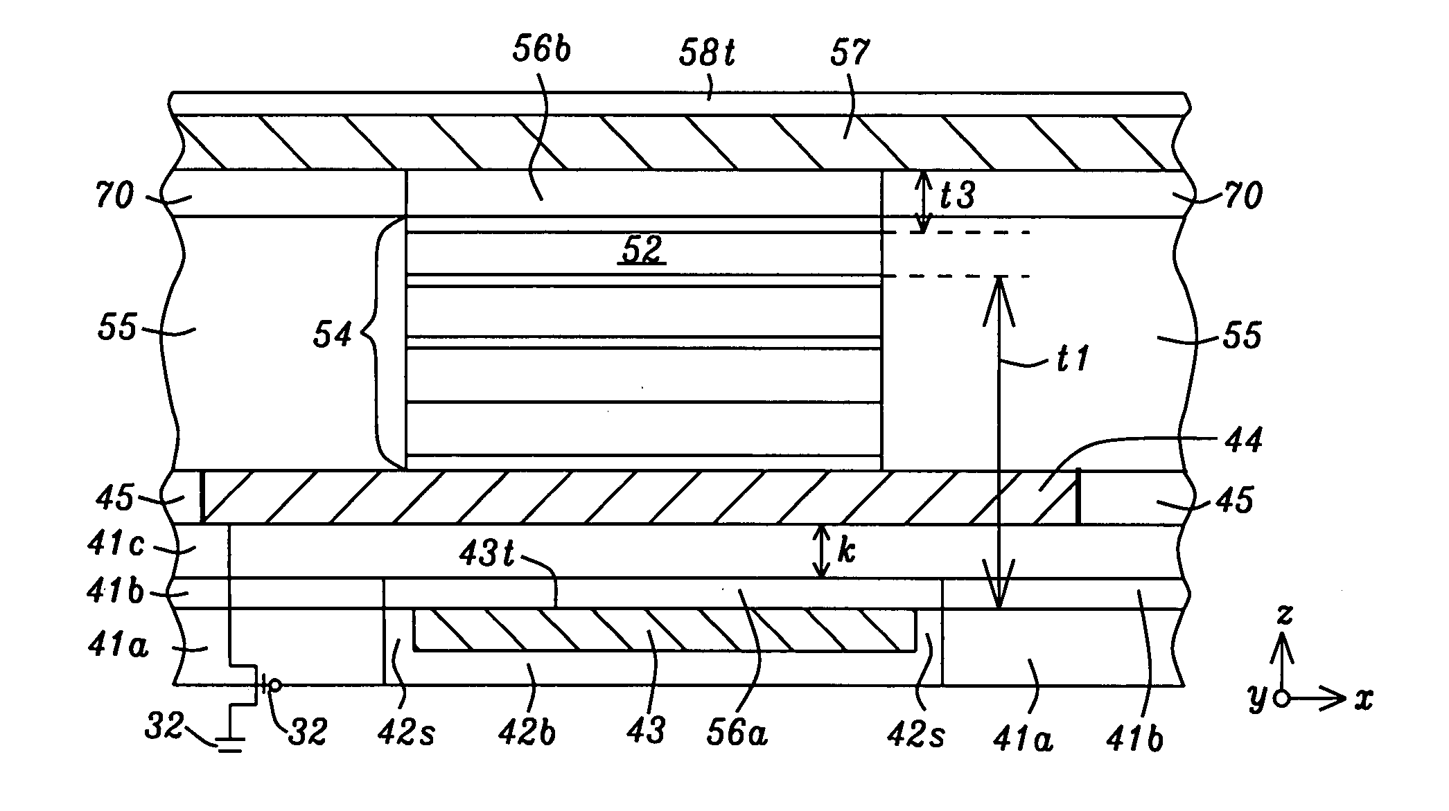
[0041]The present invention also encompasses a second embodiment wherein a spacing control layer 56 is formed between a cladded word line and a free layer in a MTJ element with a top pinned layer configuration. In FIG. 6, MRAM cell 40 is modified to show a MTJ stack of layers in which a seed layer 46, free layer 52, tunnel barrier layer 51, AP1 layer 50, coupling layer 49, AP2 layer 48, AFM layer 47, and capping layer 53 are sequentially formed with a top pinned layer structure on BE 44. Cladded bit line 57 contacts a top surface of capping layer 53. In this MRAM structure, free layer 52 is located closer to word line 42 than to bit line 57 (t58). Thus, the spacing control layer 56 is formed between word line 42 and free layer 52 in order to control the distance t5 within a certain range of 0.03 to 0.15 microns.

[0042]In the exemplary embodiment, a bottom surface of spacing control layer 56 contacts a top side 43t of word line 43 that faces BE 44. There is a thin section of dielectri...

first embodiment

[0047]A second spacing control layer 56b is formed between a top surface 53s of capping layer 53 and a side of bit line 57 facing the top surface 53s as described with respect to spacing control layer 56 in the In this case, the second spacing control layer 56b is used to control the distance s3 between bit line 57 and a top surface of free layer 52. Second spacing control layer 56b has a thickness between 0.02 and 0.12 microns to maintain a distance s3 of 0.03 to 0.15 microns between the bit line 57 and free layer 52, and is preferably comprised of the same highly conductive non-magnetic material as in spacing control layer 56 described previously.

[0048]A fourth embodiment of the present invention is depicted in FIG. 8 and represents a modification of the third embodiment where the dual pinned layer MTJ element 84 is replaced by a single pinned layer MTJ element 54. Although the exemplary embodiment depicts a bottom pinned layer configuration for MTJ 54, the present invention also...


PUM


Abstract

A cladding structure for a conductive line used to switch a free layer in a MTJ is disclosed and includes two cladding sidewalls on two sides of the conductive line, a top cladding portion on a side of the conductive line facing away from the MTJ, and a highly conductive, non-magnetic spacing control layer formed between the MTJ and conductive line. The spacing control layer has a thickness of 0.02 to 0.12 microns to maintain the distance separating free layer and conductive line between 0.03 and 0.15 microns. The spacing control layer is aligned parallel to the conductive line and contacts a plurality of MTJ elements in a row of MRAM cells. Half-select error problems are avoided while maintaining high write efficiency. A spacing control layer may be formed between a word line and a bottom electrode in a top pinned layer or dual pinned layer configuration.

Description

RELATED PATENT APPLICATION[0001]This application is related to U.S. Patent Application Publication 2008 / 0253178, Ser. No. 11 / 787,330, filing date Apr. 16, 2007; assigned to the same assignee as the current invention and which is herein incorporated by reference in its entirety.FIELD OF THE INVENTION[0002]The invention relates to an MRAM design, and in particular, to a MRAM structure wherein a spacing control layer with a tightly controlled thickness is formed between a MTJ stack of layers and a cladded bit line or cladded word line to solve the half-selected bit disturb problem without sacrificing writing efficiency. A method is also provided for fabricating the aforementioned MRAM structure.BACKGROUND OF THE INVENTION[0003]Magnetic random access memory (MRAM) that incorporates a magnetic tunneling junction (MTJ) as a memory storage cell is a strong candidate to provide a high density, fast (1-30 ns read / write speed), and non-volatile storage solution for future memory applications....

Claims


Application Information

Patent Timeline
Patent Type & Authority Applications(United States)
IPC IPC(8): H01L29/82H01L21/00
CPCB82Y25/00G11C11/16H01F10/3254H01L43/12H01L27/228H01L43/08H01F10/3263H10B61/22H10N50/10H10N50/01
Inventor MIN, TAIKAN, WAI-MING J.HEIM, DAVID E.TORNG, CHYU JIUH
Owner TAIWAN SEMICON MFG CO LTD
Why Eureka
Try Eureka