

Multi-port pumping system for substrate processing chambers
a technology of substrate processing and pumping system, which is applied in the direction of water supply installation, application, cleaning using liquids, etc., can solve the problems of limited flow capacity that cannot accommodate increased, limited rate at which the activated cleaning gas flows into the deposition chamber, and decrease in the cleaning efficiency of the activated cleaning gas
- Summary
- Abstract
- Description
- Claims
- Application Information
AI Technical Summary
Benefits of technology
Problems solved by technology
Method used
Image

Examples
Embodiment Construction
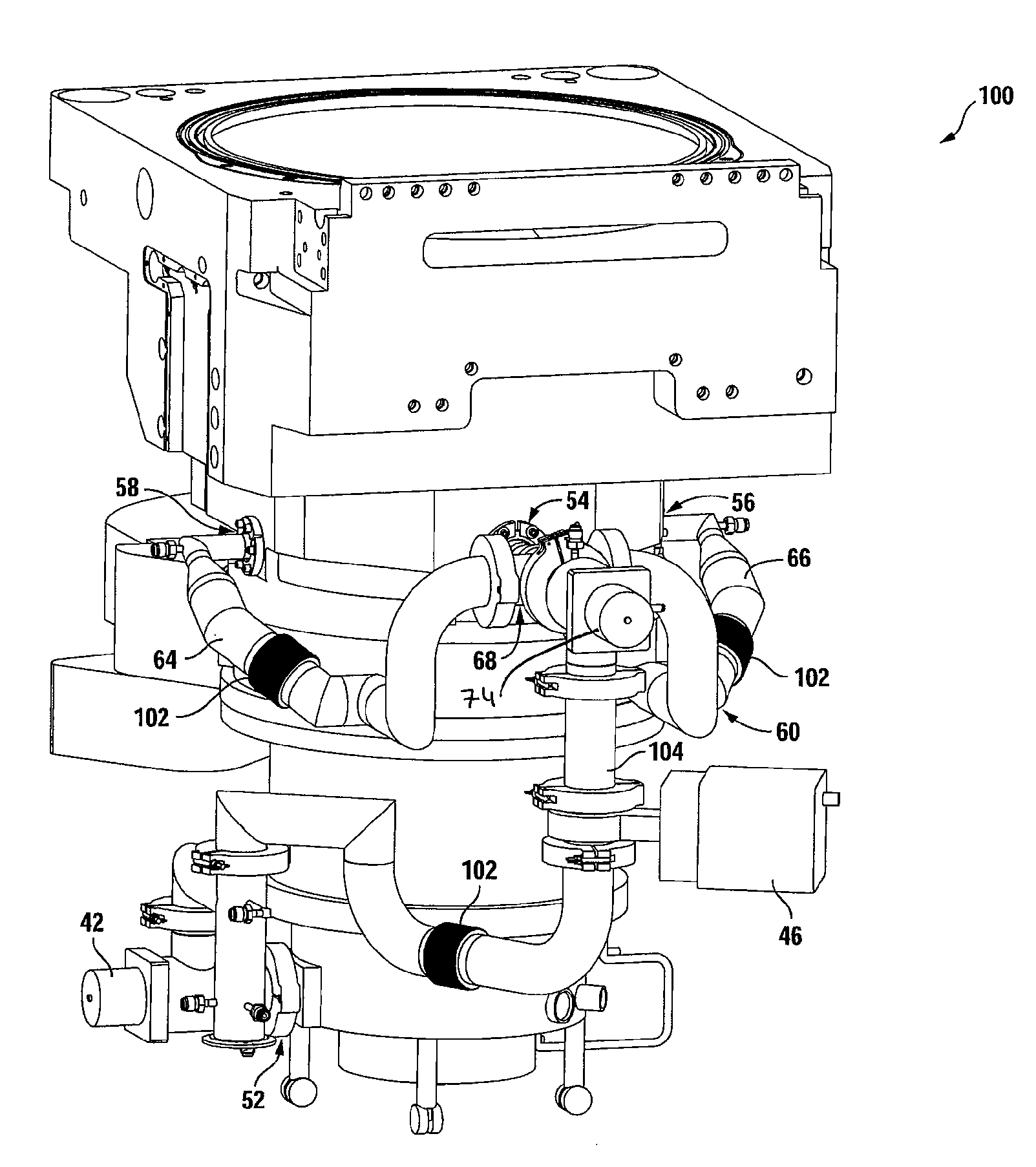
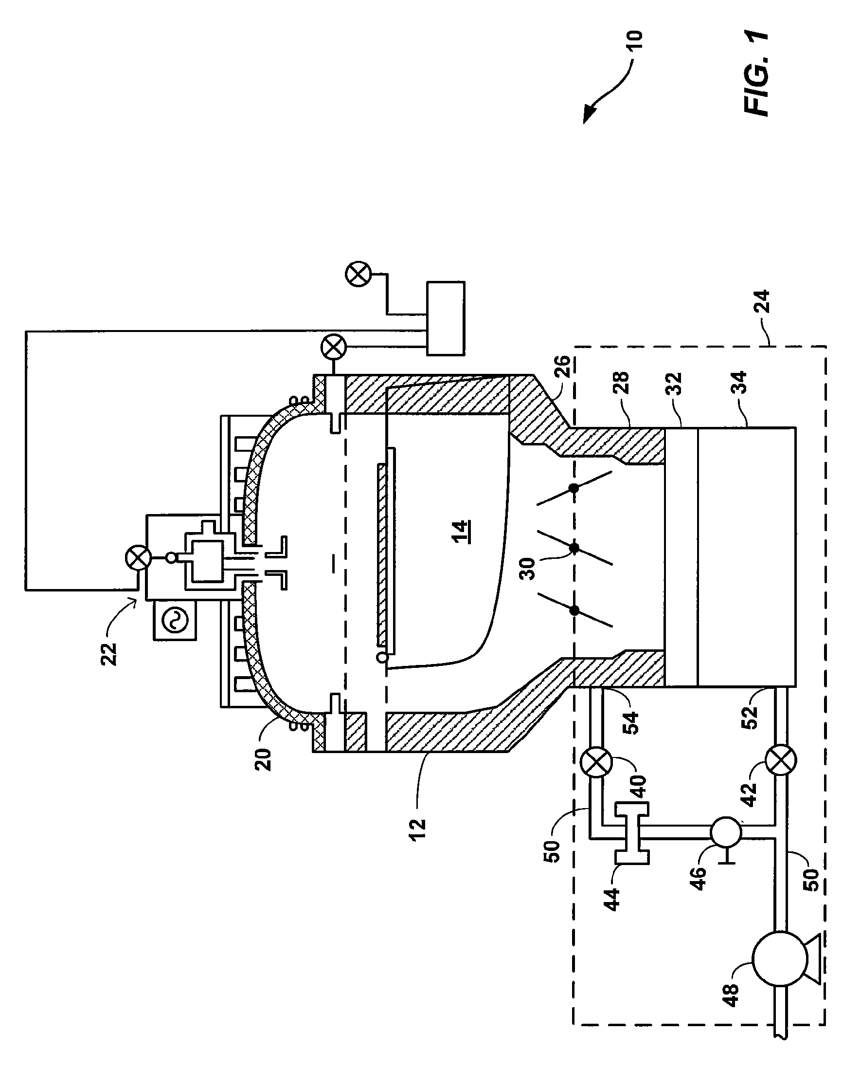
[0020]FIG. 1 is a simplified cross-sectional view of a high density plasma chemical vapor deposition (HDP-CVD) system 10 in which the techniques according to the present invention can be employed to increase the pumping capacity of system 10 during a chamber clean operation. CVD system 10 includes, among other elements, a chamber body 12, a substrate support 14 (e.g., an electrostatic chuck), gas nozzles 16, 18, a chamber dome 20, a remote plasma cleaning system 22 and a vacuum system 24. Chamber body 12, dome 20 and substrate support 14 combine to define a processing region 15 in which a substrate 2 is positioned during a substrate processing operation, such as a chemical vapor deposition operation. For convenience, numerous features of system 10 that are not directly relevant to the invention have been omitted from FIG. 1 and are not discussed herein. For example, system 10 includes a gas distribution system that delivers process gases to gas nozzles 16, 18, as well as source and ...
PUM
| Property | Measurement | Unit |
|---|---|---|
| pressure | aaaaa | aaaaa |
| pressures | aaaaa | aaaaa |
| 90° angles | aaaaa | aaaaa |
Abstract
Description
Claims
Application Information