Methods and systems of thick semiconductor drift detector fabrication

a detector and semiconductor technology, applied in the manufacture of final products, instruments, x/gamma/cosmic radiation measurement, etc., can solve the problem of limiting the practical x-ray detection efficiency to about 20 kev, and achieve better energy resolution, lower detection thresholds, and quantum efficiency. high

Inactive Publication Date: 2011-06-28
US GOVT AS REPRESENTED BY THE SEC OF THE NAVY OFFICE OF NAVAL RES NRL CODE OOCCIP
View PDF15 Cites 8 Cited by
  • Summary
  • Abstract
  • Description
  • Claims
  • Application Information

AI Technical Summary

Benefits of technology

[0004]Thick silicon drift detectors (SDDs) have better “X-ray stopping power” due to the increased silicon mass. Denser semiconductor materials such as Cadmium telluride (CdTe) and Cadmium zinc telluride (CdZnTe) have also increased X-ray stopping power in comparison to standard (thin) silicon SDDs. The advantage of the present invention over CdTe or CdZnTe based detectors is the result of a much lower noise level due to very low capacitances.
[0005]“Silicon drift detectors” have set new records as room-temperature semiconductor detectors for X- and gamma-ray spectroscopy. When compared with classical photomultiplier tubes (PMTs), SDDs offer the typical advantages of a silicon photo-detector, i.e., a higher quantum efficiency for scintillation light, the possibility of a monolithic integration of arrays of photo-detectors of almost any area and shape, and the immunity to magnetic fields. Moreover, if compared with conventional silicon pn-photo-detectors of the same active area and thickness, SDDs allow for better energy resolutions and lower detection thresholds due to the lower level of electronics noise arising from the smaller value of output capacitance.
[0006]Most SDDs have device thicknesses around 300 μm and applied voltages at the drifting cathodes 1302 range from −200 to −30 V (see FIG. 13A and 13B). A 300 μm device-thickness limits the practical x-ray detection efficiency to about 20 keV. The x-ray efficiency for 300 μm thick Si falls off rapidly above 10 keV, with 50% efficiency at 15 keV and only 9% at 30 keV. Currently, there are a large number of XRF (X-ray fluorescence) measurements that can benefit from the increase in efficiency at higher energies afforded by these new thick devices, including DoD, DoE, medical, space, and Homeland Security applications.
[0007]The general concept of a silicon drift detector (SDD) was first proposed by E. Gatti, P. F. Rehak, Nucl. Jnstrum. Methods 225, 608 (1984) and later realized by P. Rehak, J. Walton, E. Gatti, A. Longoni, M. Sampietro, J. Kemmer, H. Dietl, P. Holl, R. Klanner, G. Lutz, A. Wylie and H. Becker, Nucl. Instrum. Methods A 248, 367 (1986). In an SDD (referring to FIG. 2) two superimposed fields from the device front- and back-side direct generated electric carriers electrons 108 to a small collecting anode 206. The general electronic noise performance is improved in comparison to standard x-ray detectors because of the small size of the collecting anode 206 (low capacitance). FIG. 2 shows a first generation SDD, where drift strips 202 on the back (see back plate 210)- and front-side generate a lateral “drift-field” (see path 208) for the carrier.
[0008]Detectors with high-aspect ratio holes (or trenches) were first introduced by S. Parker, C. Kenney and J. Segal, Nucl Inst. Meths. A 395, 328 (1997) as radiation hard detectors, having vertical electrodes to deplete laterally the detector matrix—see FIG. 6A and FIG. 6B; these holes (see hole array 602) were fabricated by micro-machining techniques.
[0009]Several improvements to the SDD have been published, see e.g. L. Strüder, presentation at Advanced Instrumentation Seminars, SLAC, Stanford, [Presentation conducted Feb. 7, 2007, accessed on the Internet on Sep. 24, 2009 at: [http: / / www-group.slac.stanford.edu / ais / past SeminarDetails.asp?seminarID=60]. FIG. 3 shows a second generation silicon drift detector with an integrated Field Effect Transistor (FET) 300. The FET300, having a source 302, gate 304 and drain 306, acts as an amplifier and yields to higher resolution. FIG. 4 shows an SDD in a “bulls-eye” shape with an integrated FET 400.

Problems solved by technology

A 300 μm device-thickness limits the practical x-ray detection efficiency to about 20 keV.

Method used


Image

  • Methods and systems of thick semiconductor drift detector fabrication
  • Methods and systems of thick semiconductor drift detector fabrication
  • Methods and systems of thick semiconductor drift detector fabrication

Examples


Embodiment Construction

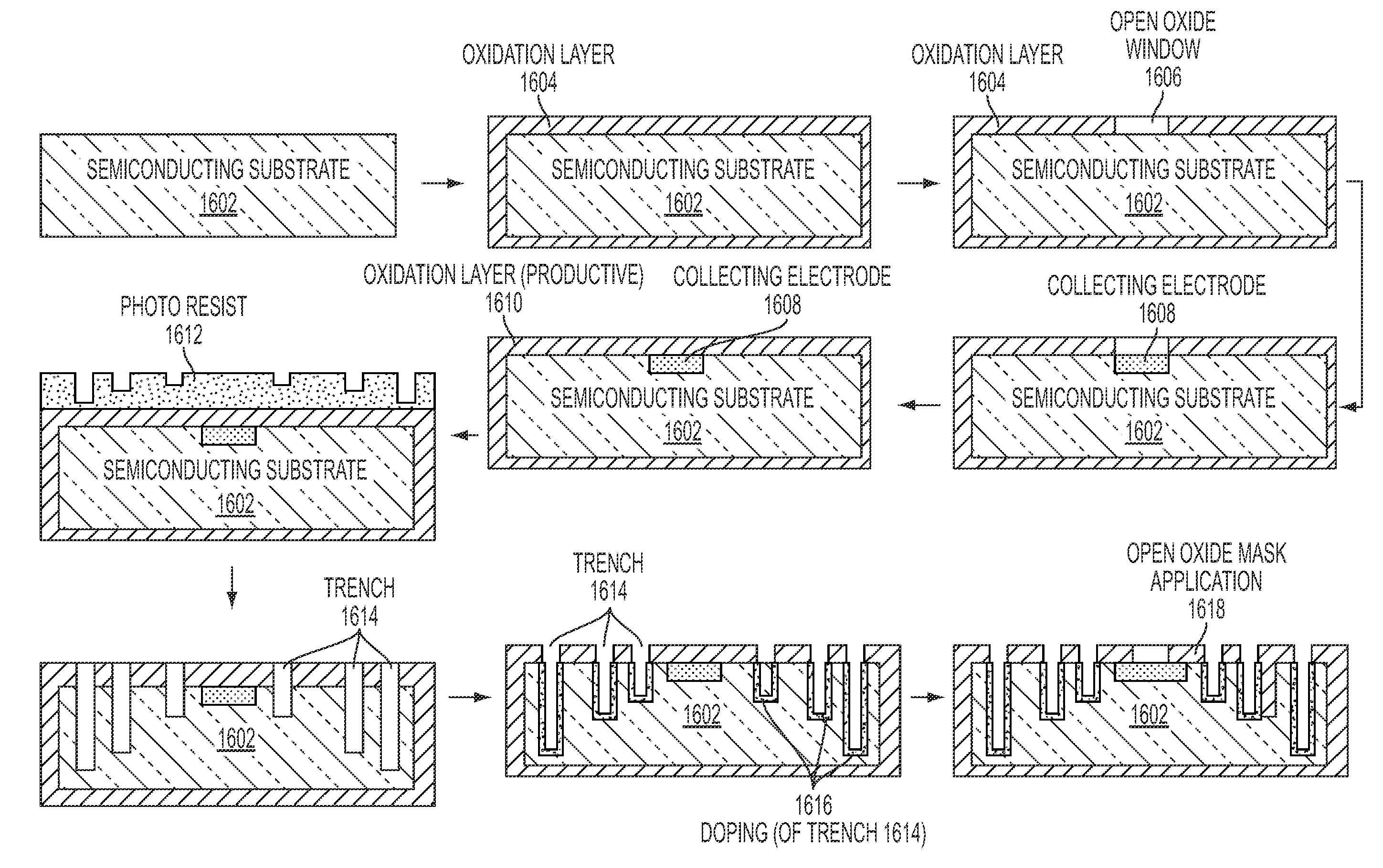
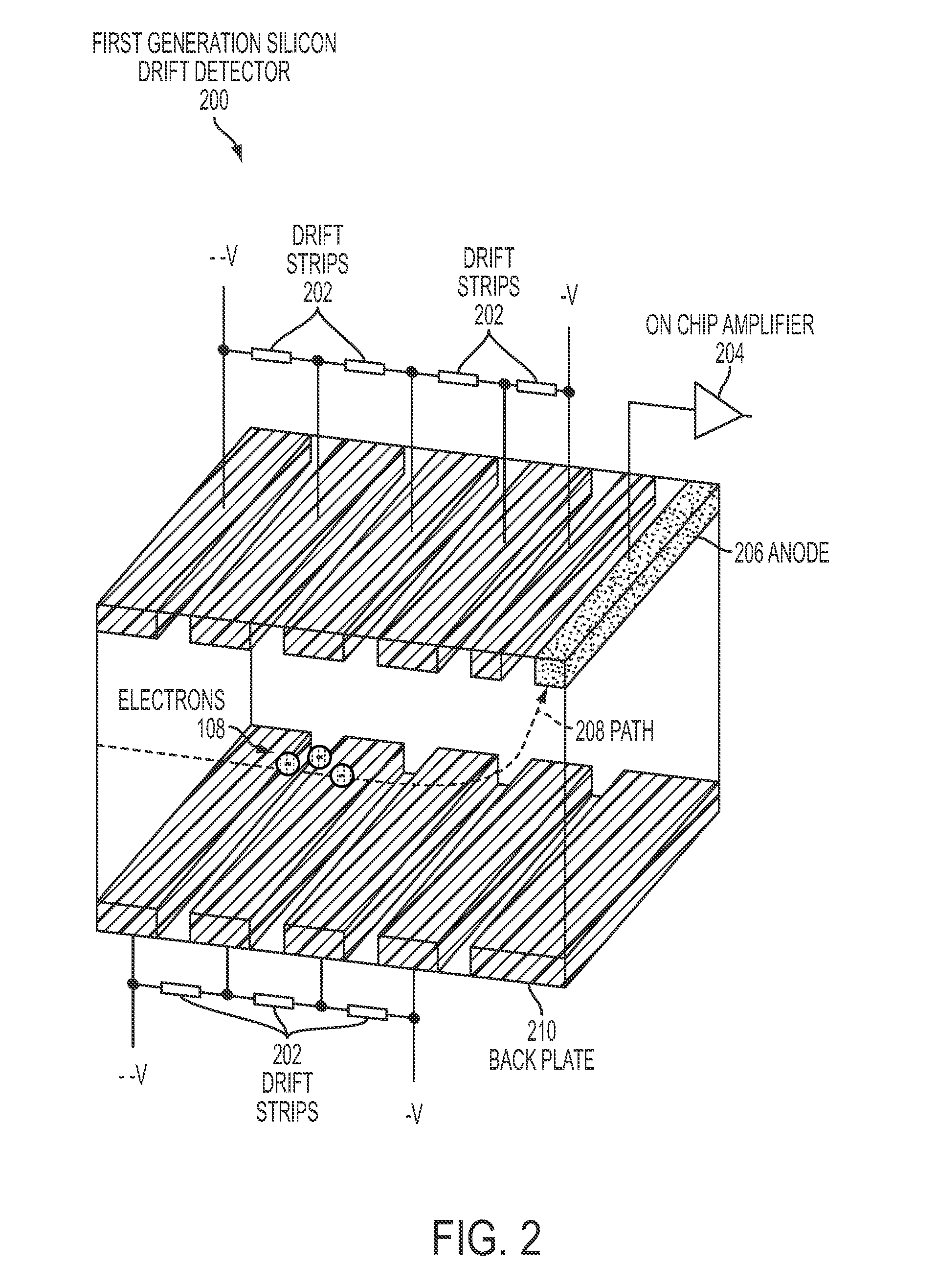
[0034]Preferred exemplary embodiments of the present invention are now described with reference to the figures, in which like reference numerals are generally used to indicate identical or functionally similar elements. While specific details of the preferred exemplary embodiments are discussed, it should be understood that this is done for illustrative purposes only. A person skilled in the relevant art will recognize that other configurations and arrangements can be used without departing from the spirit and scope of the preferred exemplary embodiments. It will also be apparent to a person skilled in the relevant art that this invention can also be employed in other applications. Further, the terms “a”, “an”, “first”, “second” and “third” etc. used herein do not denote limitations of quantity, but rather denote the presence of one or more of the referenced items(s).

[0035]In accordance with exemplary embodiments, a method and system for a process and a product are implemented in th...


PUM


Abstract

Gray-tone lithography technology is used in combination with a reactive plasma etching operation in the fabrication method and system of a thick semiconductor drift detector. The thick semiconductor drift detector is based on a trench array, where the trenches in the trench array penetrate the bulk with different depths. These trenches form an electrode. By applying different electric potentials to the trenches in the trench array, the silicon between neighboring trenches fully depletes. Furthermore, the applied potentials cause a drifting field for generated charge carriers, which are directed towards a collecting electrode.

Description

RELATED APPLICATIONS[0001]This U.S. patent application is related to U.S. provisional patent application No. 61 / 106,460 Methods and Systems of Thick Silicon Drift Detector Fabrication and to U.S. provisional patent application No. 61 / 106,417 Methods and Systems of Curved Radiation Detector Fabrication and, each provisional application having the same joint inventors and each provisional application filed on the same day (Oct. 17, 2008) are incorporated by reference herein in their entirety. Additionally, this U.S. patent application is related to U.S. patent application Ser. No. 12 / 581,469, for Methods and Systems of Curved Radiation Detector Fabrication, filed on Oct. 19, 2009 and incorporated by reference herein in its entirety. Further, this U.S. patent application is related to Patent Cooperation Treaty application PCT / US2009 / 061200, for Thick Silicon Drift Detector Fabrication and Patent Cooperation Treaty application PCT / US2009 / 061198, for Curved Radiation Detector Fabrication...

Claims


Application Information

Patent Timeline
Patent Type & Authority Patents(United States)
IPC IPC(8): H01L31/115H01L21/00
CPCH01L31/022408H01L31/1804H01L31/115Y02E10/547Y02P70/50
Inventor CHRISTOPHERSEN, MARCPHLIPS, BERNARD F.
Owner US GOVT AS REPRESENTED BY THE SEC OF THE NAVY OFFICE OF NAVAL RES NRL CODE OOCCIP
Why Eureka
Try Eureka