Supercharge Your Innovation With Domain-Expert AI Agents!

Three-stage frequency-compensated operational amplifier for driving large capacitive loads

a capacitive load, three-stage technology, applied in the direction of amplifiers, amplifiers with semiconductor devices/discharge tubes, electric devices, etc., can solve the problems of poor power supply rejection ratio (psrr) of mc amplifiers during high frequency operations, insufficient two-stage mc amplifiers for desirable operation, and all multi-stage amplifiers suffer close-loop stability problems. , to achieve the effect of low impedan

Active Publication Date: 2011-07-05
MEDIATEK SINGAPORE PTE LTD SINGAPORE
View PDF3 Cites 5 Cited by
  • Summary
  • Abstract
  • Description
  • Claims
  • Application Information

AI Technical Summary

Benefits of technology

The present invention provides a three-stage frequency-compensated operational amplifier for driving large capacitive loads. The amplifier includes a first-stage circuit, a second-stage circuit, a third-stage circuit, and a second compensation circuit. The first compensation circuit generates a first output signal by amplifying an input signal, and the second-stage circuit generates a second output signal by selectively amplifying the first output signal with a first gain while the first output signal is at a first frequency, and amplifying it with a second gain while the first output signal is at a second frequency. The third-stage circuit generates a third output signal by amplifying the second output signal. The second compensation circuit modifies the first gain to the second gain at the second frequency. The first compensation capacitor and current source are used to adjust the frequency characteristics of the second and third-stage circuits. The technical effect of this invention is to provide an improved amplifier that can drive large capacitive loads with high efficiency and accuracy.

Problems solved by technology

Since conventional cascade amplifiers, which increase the gain by stacking up transistors, are not suitable in low-voltage design due to small voltage swings, more circuit designers are aware of the importance of multi-stage amplifiers, which boost the gain by increasing the number of gain stages horizontally.
However, all multi-stage amplifiers suffer close-loop stability problems due to their multiple-pole nature in the small-signal transfer functions.
In addition, the MC amplifier 100 has a poor power supply rejection ratio (PSRR) during high frequency operations.
Therefore, if a good PSRR is required, the two-stage MC amplifier 10 is insufficient for desirable operation.
Therefore, the bandwidth of the NMC amplifier 20 is poor.
Moreover, the NMC amplifier 20 is not suitable for low-power design since the previously stated assumption gm3>>gm1 and gm2 may not be valid.
However, the two-stage Ahuja compensation amplifier 30 fails to achieve good compensation in certain cases.

Method used


Image

  • Three-stage frequency-compensated operational amplifier for driving large capacitive loads
  • Three-stage frequency-compensated operational amplifier for driving large capacitive loads
  • Three-stage frequency-compensated operational amplifier for driving large capacitive loads

Examples


first embodiment

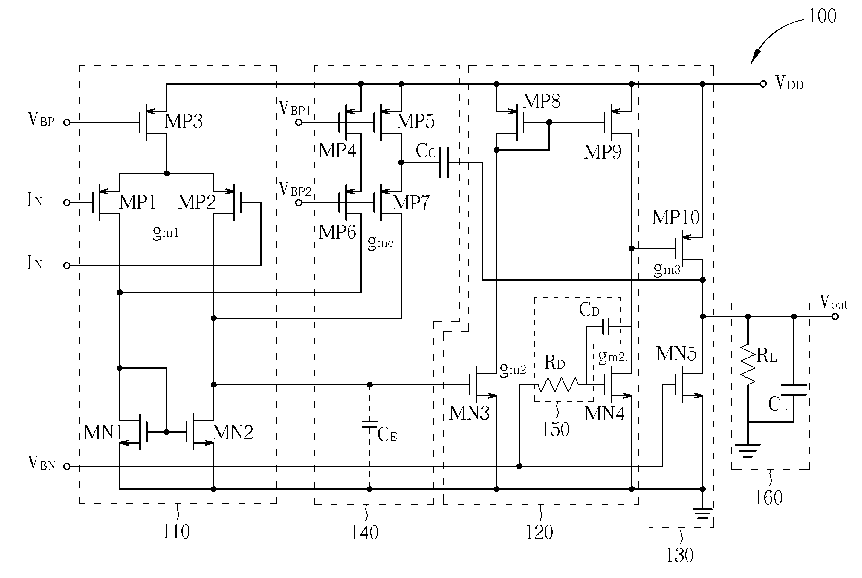
[0041]Reference is made to FIG. 6 for a diagram of a three-stage operational amplifier 100 according to the present invention. In the operational amplifier 100, the first stage circuit 110 includes transistors MP1-MP3, MN1 and MN2. The second stage circuit 120 includes transistors MP8, MP9, MN3 and MN4. The third stage circuit 130 includes transistors MP10 and MN5. The Ahuja compensation circuit 140 includes transistors MP4-MP7 and compensation capacitors CC and CE. VDD, VBP, VBN, VBP1, and VBN2 are bias voltages for operating the operational amplifier 100. Meanwhile, the transconductance of the first stage circuit 110 contributed by the transistors MP1 and MP2 is represented by gm1; the transconductance of the second stage circuit 120 contributed by the transistor MN3 is represented by gm2; the transconductance of the second stage circuit 120 contributed by the transistor MN4 is represented by gm21; the transconductance of the third stage circuit 130 contributed by the transistor M...

second embodiment

[0061]The class AB configuration is sometimes referred to as a “push-pull” configuration since a first branch of the output stage “pushes” or sources currents to a load while a second branch of the output stage “pulls” or sinks current from the load. Class-AB amplifiers can reduce high power consumption of a class-A amplifier by always having one output branch substantially turned off when the other output branch is turned on. Although the current in one leg of a class AB amplifier is substantially turned off there is a small amount of current flowing in that leg. The small residual current in the class AB amplifier avoids the crossover distortion produced the turning on and off of the currents in class-B amplifiers. By employing the class AB output stage scheme, the operational amplifier 200 according to the present invention can achieve better power efficiency while driving heavy resistive loads.

[0062]Please refer to FIG. 9 for a diagram of a three-stage operational amplifier 400 ...

fourth embodiment

[0068]Similarly, for the present invention depicted in FIG. 9, the PSRRVDD4 and PSRRGND4 of the second stage circuit 124 in isolation can be represented by:

[0069]PSRRVDD⁢⁢4=(ro⁢⁢8-ro⁢⁢9)⁢ro⁢⁢5A2⁡(ro⁢⁢5+ro⁢⁢9)⁢ro⁢⁢8(10)PSRRGND⁢⁢4=(ro⁢⁢8+r59)⁢ro⁢⁢9A2⁡(ro⁢⁢5+ro⁢⁢9)⁢ro⁢⁢8(11)

[0070]where ro8 is the small signal drain resistance of the transistor MP8;

[0071]ro9 is the small signal drain resistance of the transistor MP9;

[0072]ro5 is the small signal drain resistance of the transistors MN8 and MN9 coupled in parallel; and

[0073]A2 is the DC gain of the second stage circuit 124

[0074]From (8) and (10), the second stage circuit 124 can have a better (lower) VDD-PSRR since the numerator of PSRRVDD4 can be adjusted to zero, which happens when the disturbance current transmitted through the transistor MP9 (after being mirrored and phase-inverted by the transistor MN7) matches the disturbance current transmitted through the transistor MP8 (after being mirrored and phase-inverted by the transistor MN...


PUM


Abstract

A three-stage frequency-compensated operational amplifier includes a first-stage circuit, a second-stage circuit incorporated with a first compensation circuit, a third-stage circuit, and a second compensation circuit. The three-stage frequency-compensated operational amplifier functions as a two-stage operational amplifier at high frequencies, thereby capable of driving large capacitive loads with low power consumption.

Description

CROSS REFERENCE TO RELATED APPLICATIONS[0001]This application claims the benefit of U.S. Provisional Application No. 61 / 097,202, filed on Sep. 15, 2008 and entitled “Ahuja Frequency Compensation for 3-stage Operational Amplifiers”, the contents of which are incorporated herein by reference.BACKGROUND OF THE INVENTION[0002]1. Field of the Invention[0003]The present invention relates to an operational amplifier, and more particularly, to an operational amplifier capable of driving large capacitive loads with low power consumption.[0004]2. Description of the Prior Art[0005]Operational amplifiers have been applied extensively in the field of electrical devices and electronics, such as inverter amplifiers, integrators, and filter circuits, to name just a few instances. With the rapid scaling in CMOS processes, supply voltages in VLSL have been dramatically reduced in recent years. Acting as a fundamental block in most analog systems, operational amplifiers are required to achieve high ga...

Claims


Application Information

Patent Timeline
Patent Type & Authority Patents(United States)
IPC IPC(8): H03F1/14
CPCH03F1/086H03F3/45192H03F2200/153H03F2200/45H03F2203/45632H03F2203/45674
Inventor DASGUPTA, UDAY
Owner MEDIATEK SINGAPORE PTE LTD SINGAPORE
Features
  • R&D
  • Intellectual Property
  • Life Sciences
  • Materials
  • Tech Scout
  • Unparalleled Data Quality
  • Higher Quality Content
  • 60% Fewer Hallucinations
Learn More