
Plasma display panel having laminated dielectric layer

a dielectric layer and plasma display technology, applied in the direction of gas discharge filling, gas discharge vessel/container, gas discharge tube, etc., can solve the problem of inability to have adequate resistance to the applied voltage, and achieve the effect of enhancing the voltage resistance properties of the dielectric layer

Inactive Publication Date: 2011-07-12
PANASONIC CORP
View PDF18 Cites 0 Cited by
  • Summary
  • Abstract
  • Description
  • Claims
  • Application Information

AI Technical Summary

Benefits of technology

"The present invention provides a PDP with improved voltage resistance properties and reduced electric power consumption. This is achieved by depositing a first dielectric layer with small nano-particles and a second dielectric layer with larger nano-particles or leadless glass material. The second dielectric layer has a lamination structure made up of a small nano-particle layer and a larger nano-particle layer or leadless glass material layer. The second dielectric layer is formed of a small nano-particle silica film and a larger nano-particle silica film or leadless glass material layer. This prevents cracks in the small nano-particle silica film and improves the product yield in the manufacturing process. The second dielectric layer has a thickness ranging from 3 μm to 20 μm. The PDP also includes discharge electrodes with bus electrodes and transparent electrodes, and the second dielectric layer overlies the full face of the first dielectric layer or a portion of the second dielectric layer facing the bus electrodes. The second and third dielectric layers are both formed of leadless glass material. The discharge gas preferably includes 15% or more of xenon to improve the luminous efficiency of the PDP."

Problems solved by technology

However, the dielectric layer formed of the conventional composition including nanosized particles is a porous dielectric layer of a single layer structure, and has the disadvantage of being incapable of having adequate resistance to the applied voltage.

Method used


Image

  • Plasma display panel having laminated dielectric layer
  • Plasma display panel having laminated dielectric layer
  • Plasma display panel having laminated dielectric layer

Examples


first embodiment

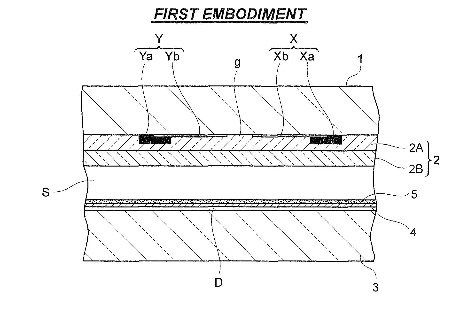
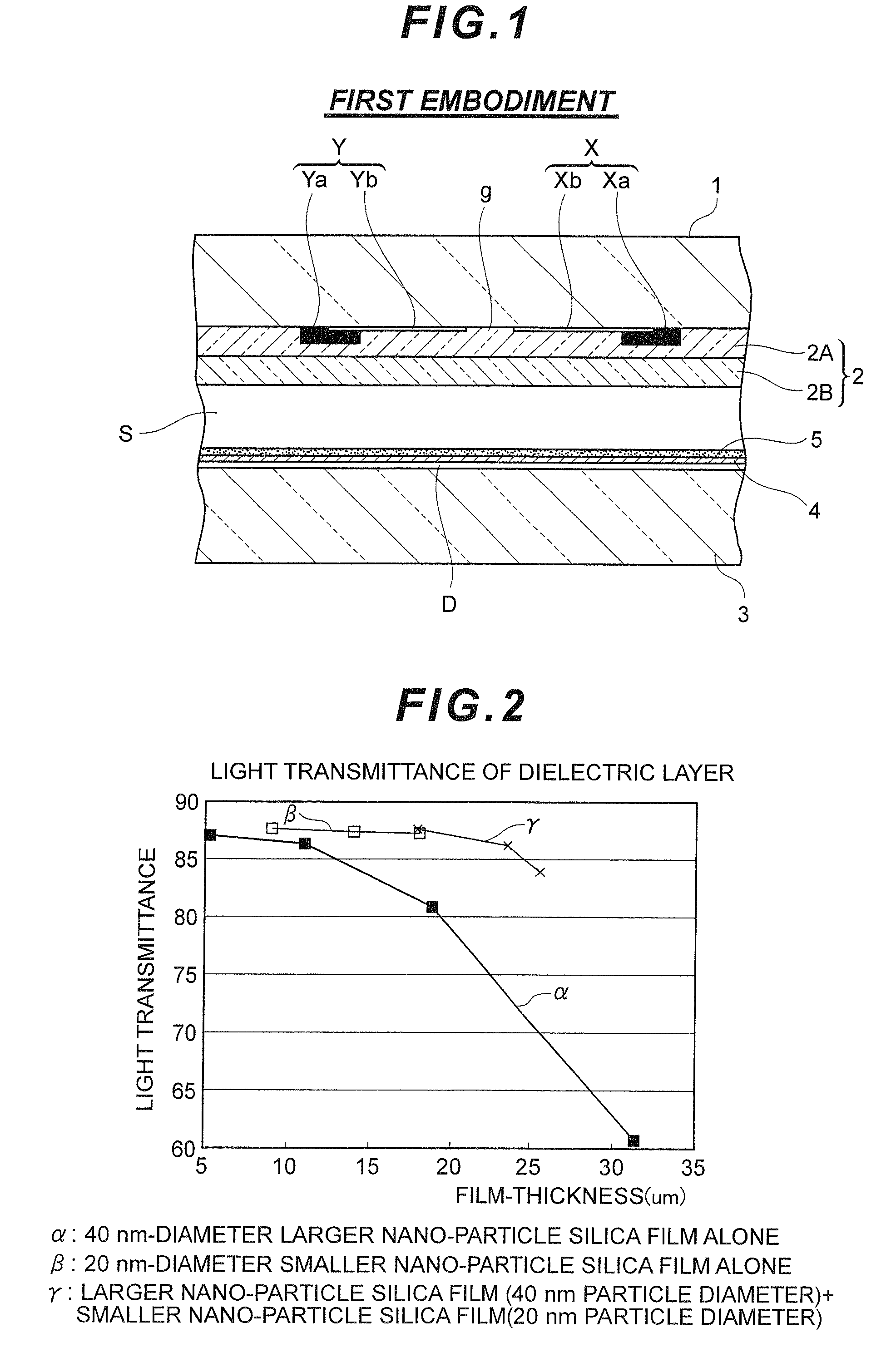
[0043]FIG. 1 is a sectional view illustrating a first embodiment of the exemplary embodiments of the PDP according to the present invention.

[0044]In FIG. 1, a plurality of row electrode pairs (X, Y), each extending in the row direction (the direction at right angles to the drawing in FIG. 1), are arranged parallel to each other in the column direction (the right-left direction in FIG. 1) on the inner face of the front glass substrate 1 which form part of the panel screen.

[0045]Each of the face-to-face row electrodes X, Y constituting each of the row electrode pairs (X, Y) is composed of a metal-formed bus electrode Xa (Ya) and a transparent electrode Xa (Ya). The transparent electrodes Xb and Yb in each row electrode pair (X, Y) extend out from the respective bus electrodes Xa and Ya so as to face each other across a discharge gap g.

[0046]In turn, a dielectric layer 2 is deposited on the inner face of the front glass substrate 1 so as to overlie the row electrode pairs (X, Y).

[0047]...

second embodiment

[0073]FIG. 4 is a sectional view illustrating a second embodiment of the exemplary embodiments of the PDP according to the present invention.

[0074]The structure of the PDP of the second embodiment is the same as that of the PDP described in the first embodiment, except for a dielectric layer 12 covering the row electrode pairs (X, Y) deposited on the inner face of the front glass substrate 1, and the same components as those in the PDP of the first embodiment are designated in FIG. 4 with the same reference numerals as in FIG. 1.

[0075]In FIG. 4, the dielectric layer 12 has a double layer structure made up of a first dielectric layer 12A directly covering the row electrode pairs (X, Y) arranged on the inner face of the front glass substrate 1, and a second dielectric layer 12B deposited on the first dielectric layer 12A.

[0076]The first dielectric layer 12A comprises a smaller nano-particle silica film formed of nano-particle silica having a particle diameter from 10 nm to 25 nm as in...

third embodiment

[0094]FIG. 7 is a sectional view illustrating a third embodiment of the exemplary embodiments of the PDP according to the present invention.

[0095]The structure of the PDP of the third embodiment is the same as that of the PDP described in the first embodiment, except for a dielectric layer 22 covering the row electrode pairs (X, Y) deposited on the inner face of the front glass substrate 1, and the same components as those in the PDP of the first embodiment are designated in FIG. 7 with the same reference numerals as in FIG. 1.

[0096]FIG. 7 only illustrates the structure of an area of the front glass substrate 1 in which the row electrode X of the row electrode pair (X, Y) is provided. The structure of the area around the row electrode X will be described below, and the same can be said of the area around the row electrode Y.

[0097]In FIG. 7, the dielectric layer 22 has a double layer structure made up of a first dielectric layer 22A directly covering the row electrode pairs (X, Y) ar...


PUM

PropertyMeasurementUnit
particle diameteraaaaaaaaaa
light transmittanceaaaaaaaaaa

Abstract

A PDP is equipped with row electrode pairs deposited on the inner face of a front glass substrate and a dielectric layer covering the row electrode pairs. A discharge space defined between the front glass substrate and the back glass substrate is filled with a discharge gas. The dielectric layer has a laminated structure made up of a first dielectric layer formed of a smaller nano-particle silica film including silica particles of a particle diameter of 10 nm to 25 nm, and a second dielectric layer formed of a larger nano-particle silica film including silica particles of a particle diameter of 25 nm to 40 nm.

Description

BACKGROUND OF THE INVENTION[0001]1. Field of the Invention[0002]This invention relates to a structure of plasma display panels.[0003]The present application claims priority from Japanese Application No. 2007-185447, the disclosure of which is incorporated herein by reference.[0004]2. Description of the Related Art[0005]A plasma display panel (hereinafter referred to as “PDP”) typically comprises a front glass substrate on the inner face of which a plurality of row electrode pairs are provided. The row electrode pairs each extend in a direction at right angles to column electrodes that are provided on a back glass substrate facing the front glass substrate across a discharge space. In this manner, discharge cells arranged in a matrix are formed in the respective positions in the discharge space corresponding to the intersections between the row electrode pairs and the column electrode. Thus, a discharge is initiated between one row electrode in the row electrode pair and the column e...

Claims


Application Information

Patent Timeline
Patent Type & Authority Patents(United States)
IPC IPC(8): H01J17/49H01J11/22H01J11/24H01J11/34H01J11/38H01J11/50
CPCH01J11/12H01J11/38
Inventor OKADA, TAKERUKAWAI, KENJI
Owner PANASONIC CORP
Learn More