Information display panel and method for manufacturing the same

a technology of information display panel and display panel, which is applied in the field of information display panel, can solve the problems of slow response rate, lack of imaging repetition stability, and difficulty in maintaining a stable dispersion sta

Inactive Publication Date: 2011-07-12
BRIDGESTONE CORP
View PDF7 Cites 2 Cited by
  • Summary
  • Abstract
  • Description
  • Claims
  • Application Information

AI Technical Summary

Benefits of technology

[0009]The present invention has for its object to eliminate the drawbacks mentioned above and to provide an information display panel, which can improve a flexibility of the rear substrate with the electrode by an inexpensive cost, achieve an easy handling of the substrate and decrease a panel breakage due to a detachment of two substrates.
[0011]The present invention has for its another object to provide an information display panel, which can be obtained inexpensively since the number of parts can be decreased, and take no trouble for manufacturing since the number of mounting processes can be decreased.
[0014]According to the invention, since the rear substrate is constituted by a flexible material, and a metal electrode is formed on the rear substrate by a patterning process using a vapor deposition and a sputtering or a metal electrode is formed on the rear substrate by effecting a patterning process to a metal film formed by a vapor deposition or a sputtering, it is possible to obtain the information display panel, which can improve a flexibility of the rear substrate, achieve an easy handling of the substrate and decrease a panel breakage due to a detachment of two substrates. Moreover, a metal especially aluminum is an inexpensive electrode material, which can be formed by a vapor deposition or a sputtering, and a patterning process such as etching can be easily performed thereto. Further, if it is combined with the rear substrate made of a resin material especially PET or PEN, it is possible to obtain the flexible rear substrate in an extremely inexpensive manner. In this manner, according to the invention, it is possible to decrease a cost of the information display panel.
[0015]As a preferred embodiment for achieving the another object mentioned above, since the rear substrate is constituted by a flexible material, and a metal electrode is formed on the rear substrate by a patterning process using a vapor deposition and a sputtering or a metal electrode is formed on the rear substrate by effecting an etching process to a metal film formed by a vapor deposition or a sputtering, a flexibility of the substrate and the electrode required for mounting the chip can be obtained, and thus a chip of information display driver and so on can be directly mounted on the rear substrate. As a result, it is possible to obtain an information display panel, which can be obtained inexpensively since the number of parts can be decreased, and take no trouble for manufacturing since the number of mounting processes can be decreased.
[0019]According to the method of manufacturing the information display panel of the invention, when the chip of information display driver and so on is directly mounted on the rear substrate, the chip and the metal electrode formed on the rear substrate are directly connected by applying an ultrasonic wave and a pressure thereto through a wiring extended from the metal electrode. Therefore, a connection due to a metal eutectic crystal by means of an ultrasonic wave can be performed between the wiring and the terminal, and thus it is possible to obtain the information display panel and the method of manufacturing the information display panel, in which the chip of information display driver and so on can be directly mounted on the substrate even in the case of using the inexpensive substrate having a low heat resistance.

Problems solved by technology

However, in the electrophoresis method, there is a problem that a response rate is slow by the reason of viscosity resistance because the particles migrate among the electrophoresis solution.
Further, there is a problem of lacking imaging repetition stability, because particles with high specific gravity of titanium oxide is scattered within solution of low specific gravity, it is easy to subside, difficult to maintain a stability of dispersion state.
Even in the case of microencapsulating, cell size is diminished to a microcapsule level in order to make it hard to appear, however, an essential problem was not overcome at all.
[The Imaging Society of Japan “Japan Hardcopy '99” (Jul. 21-23, 1999) Transaction Pages 249-252] However, there are some problems on this method: such that a construction becomes complicated since it is necessary to provide the charge transport layer, further a charge generation layer; and such that a display stability is deteriorated since it is difficult to constantly inject a charge in a conductive particle.
In this case, according to a condition of the rear substrate, there are drawbacks, such that a handling of the rear substrate is difficult since an electrode arranged to the substrate is peeled off, and such that the panel becomes easy to break since two substrates are detached due to a stress acting for the information display panel obtained by laminating two substrates by adhesives.
Particularly, in the information display panel such as an electric paper, in which a display surface is sometimes bended, the above problems occur remarkably.
However, both of the glass material and the ITO material have a low flexibility, and thus they can't overcome the above problems.
In addition, they are expensive and there is a drawback such that a cost of the information display panel becomes high.

Method used


Image

  • Information display panel and method for manufacturing the same
  • Information display panel and method for manufacturing the same
  • Information display panel and method for manufacturing the same

Examples


examples

[0094]Hereinafter, the present invention will be explained further specifically with reference to the examples according to the invention and the comparative examples, but the present invention is not limited to the following examples.

[0095]

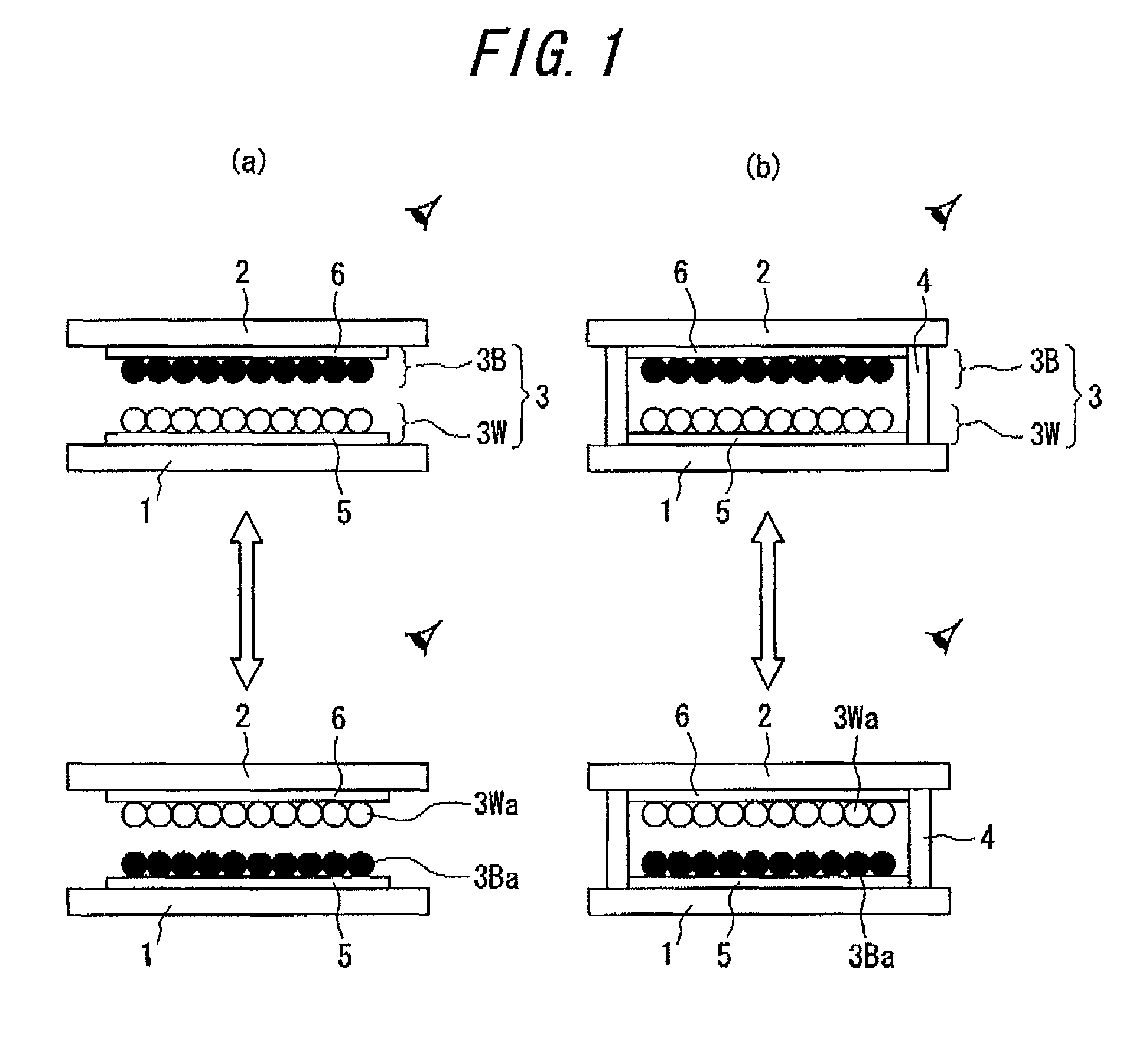
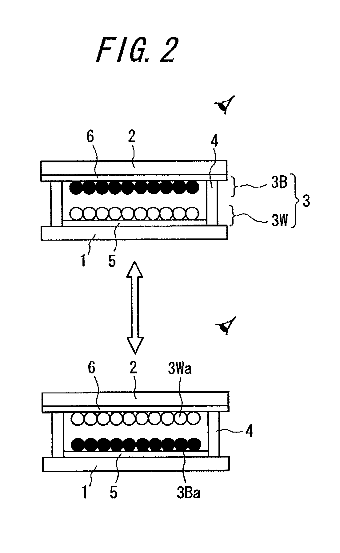
(As to a Relation Between the Rear Substrate and the Electrode)

[0096]An example 1 in which an electrode 205 was formed by vapor-depositing aluminum (Al) on a rear substrate 201 made of PET, an example 2 in which the electrode 205 was formed by sputtering aluminum (Al) on the rear substrate 201 made of PET, and a comparative example 1 in which the electrode 205 was formed by a patterning process in such a manner that ITO was formed on the rear substrate 201 made of PET by means of a photolithograph method, were prepared. In respective examples, a thickness of the rear substrate was set to 100 μm and a thickness of the electrode was set to 0.06 μm. Actually, as shown in FIG. 9, the electrode having a predetermined pattern was formed on the rear sub...


PUM

PropertyMeasurementUnit
thicknessaaaaaaaaaa
thicknessaaaaaaaaaa
temperatureaaaaaaaaaa

Abstract

In an information display panel, in which display media are sealed between a transparent front substrate and a rear substrate, and, in which the display media, to which an electrostatic field is applied from electrodes arranged respectively to the front substrate and the rear substrate, are made to move so as to display information such as an image, the rear substrate is constituted by a flexible material, and a metal electrode is formed on the rear substrate by a patterning process using a vapor deposition and a sputtering or a metal electrode is formed on the rear substrate by effecting a patterning process to a metal film formed by a vapor deposition or a sputtering. In this manner, it is possible to obtain an information display panel, which can improve a flexibility of the rear substrate with the electrode by an inexpensive cost, achieve an easy handling of the substrate and decrease a panel breakage due to a detachment of two substrates.

Description

TECHNICAL FIELD[0001]The present invention relates to an information display panel, in which display media are sealed between a transparent front substrate and a rear substrate, and, in which the display media, to which an electrostatic field is applied from electrodes arranged respectively to the front substrate and the rear substrate, are made to move so as to display information such as an image, and a method of manufacturing the same.RELATED ART[0002]As an information display device substitutable for liquid crystal display (LCD), information display devices with the use of technology such as an electrophoresis method, an electro-chromic method, a thermal method, a dichroic-particles-rotary method and so on are proposed.[0003]As for these information display devices, it is conceivable as inexpensive visual display device of the next generation from a merit having wide field of vision close to normal printed matter, having smaller consumption, or having a memory function, as compa...

Claims


Application Information

Patent Timeline
Patent Type & Authority Patents(United States)
IPC IPC(8): G02B26/00G09G3/34G02F1/167
CPCG02F1/133305G02F1/167G02F1/1345
Inventor SAKURAI, RYO
Owner BRIDGESTONE CORP
Why Eureka
Try Eureka