Multi-serial interface stacked-die memory architecture

a memory architecture and serial interface technology, applied in multiplex communication, data switching networks, instruments, etc., can solve the problems of limiting the number of memory cards or modules, and often mismatching performance between modern host processors, etc., to achieve parallelism, increase the density of memory systems, and improve the effect of memory density

Active Publication Date: 2011-07-12
MICRON TECH INC
View PDF33 Cites 105 Cited by
  • Summary
  • Abstract
  • Description
  • Claims
  • Application Information

AI Technical Summary

Problems solved by technology

As a result, a mis-match in performance often exists between the modern host processor and the semiconductor memory subsystem to which the processor is mated to receive instructions and data.
However, current-technology memory subsystems often represent a compromise between performance and density.
Higher bandwidths may limit the number of memory cards or modules that may be connected in a system without exceeding Joint Electron Device Engineering Council (JEDEC) electrical specifications.
Extensions to JEDEC interface standards such as dynamic data rate (DDR) synchronous dynamic random access memory (SDRAM) have been proposed but may be generally found lacking as to future anticipated memory bandwidths and densities.
Weaknesses include lack of memory power optimization and the uniqueness of the interface between the host processor and the memory subsystem.
The latter weakness may result in a need to redesign the interface as processor and / or memory technologies change.

Method used


Image

  • Multi-serial interface stacked-die memory architecture
  • Multi-serial interface stacked-die memory architecture
  • Multi-serial interface stacked-die memory architecture

Examples


Embodiment Construction

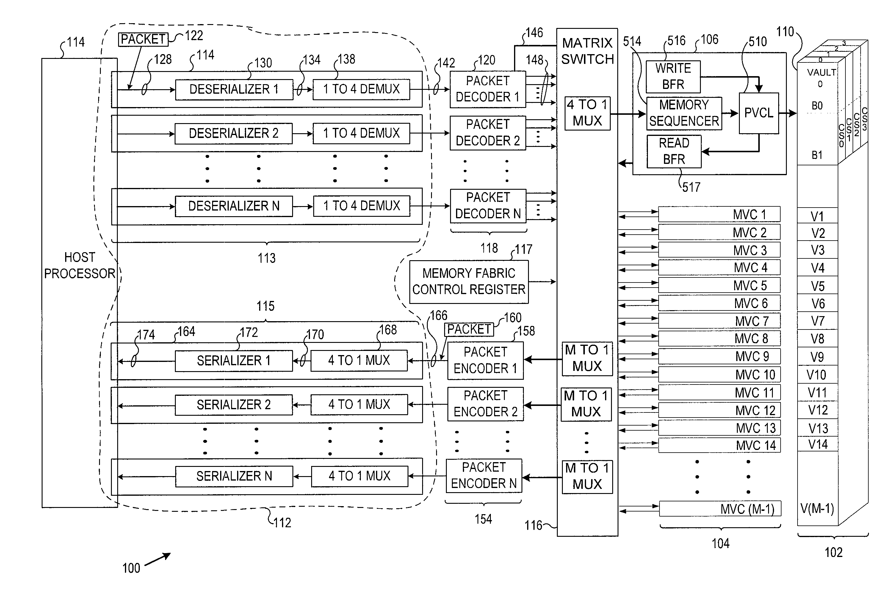
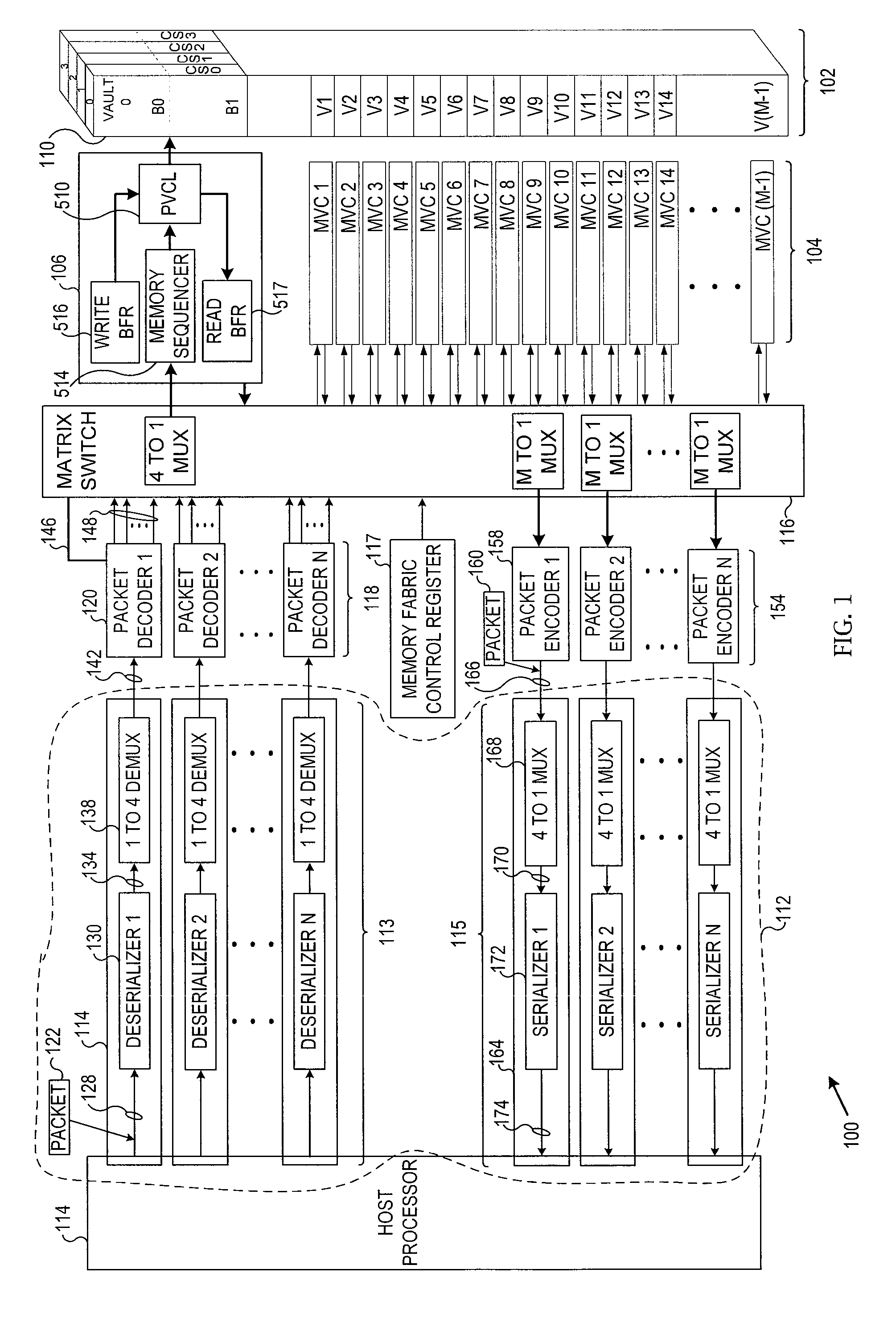
[0012]FIG. 1 is a block diagram of a memory system 100 according to various example embodiments of the current invention. The memory system 100 operates to substantially concurrently transfer a plurality of outbound and / or inbound streams of commands, addresses, and / or data between one or more originating devices and / or destination devices (e.g., one or more processors) and a set of stacked-array memory “vaults.” Increased memory system density, bandwidth, parallelism, and scalability may result.

[0013]Multi-die memory array embodiments herein aggregate control logic that is normally located on each individual memory array die in previous designs. Subsections of a stacked group of dies, referred to herein as a “memory vault,” share common control logic. The memory vault architecture strategically partitions memory control logic to increase energy efficiency while providing a finer granularity of powered-on memory banks. Embodiments herein also enable a standardized host processor to ...


PUM


Abstract

Systems and methods disclosed herein substantially concurrently transfer a plurality of streams of commands, addresses, and / or data across a corresponding plurality of serialized communication link interfaces (SCLIs) between one or more originating devices or destination devices such as a processor and a switch. At the switch, one or more commands, addresses, or data corresponding to each stream can be transferred to a corresponding destination memory vault controller (MVC) associated with a corresponding memory vault. The destination MVC can perform write operations, read operations, and / or memory vault housekeeping operations independently from concurrent operations associated with other MVCs coupled to a corresponding plurality of memory vaults.

Description

RELATED APPLICATIONS[0001]This application is a continuation-in-part of U.S. application Ser. No. 12 / 166,814 which was filed Jul. 2, 2008, U.S. application Ser. No. 12 / 166,871 which was filed Jul. 2, 2008 and U.S. application Ser. No. 12 / 176,951 which was filed on Jul. 21, 2008.TECHNICAL FIELD[0002]Various embodiments described herein relate to apparatus, systems, and methods associated with semiconductor memories, including stacked-die memory architectures.BACKGROUND INFORMATION[0003]Microprocessor technology has evolved at a faster rate than that of semiconductor memory technology. As a result, a mis-match in performance often exists between the modern host processor and the semiconductor memory subsystem to which the processor is mated to receive instructions and data. For example, it is estimated that some high-end servers idle three out of four clocks waiting for responses to memory requests.[0004]In addition, the evolution of software application and operating system technolog...

Claims


Application Information

Patent Timeline
Patent Type & Authority Patents(United States)
IPC IPC(8): H04L12/28H04J3/00G06F13/00G06F13/28G11C11/00
CPCG06F13/4022G06F13/1684G06F13/1668Y02B60/1235G06F2213/16Y02B60/1228Y02D10/00G06F13/14G11C7/10
Inventor JEDDELOH, JOE M.LABERGE, PAUL A.
Owner MICRON TECH INC
Why Eureka
Try Eureka