
Read and match circuit for low-voltage content addressable memory

a low-voltage content and addressable memory technology, applied in the logic circuit, information storage, static storage, etc., can solve the problems of increased noise, decreased static noise margin, and damage to stored data, and achieve the effect of increasing the static noise margin of reading stored signals of memory cells and improving stability

Inactive Publication Date: 2011-08-16
NATIONAL CHUNG CHENG UNIV
View PDF4 Cites 1 Cited by
  • Summary
  • Abstract
  • Description
  • Claims
  • Application Information

AI Technical Summary

Benefits of technology

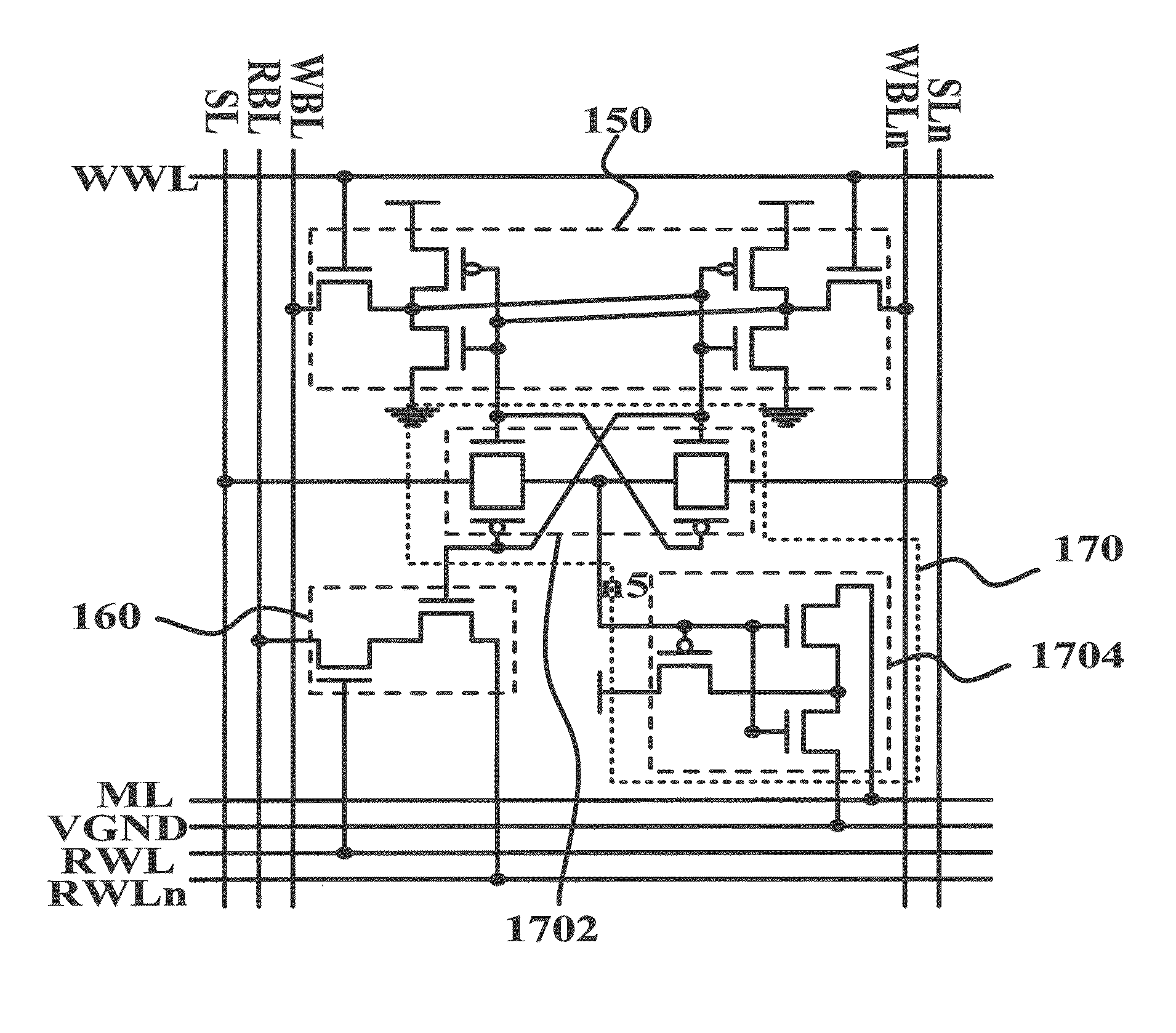
[0009]The primary objective of the present invention is to provide a read and match circuit for a low-voltage content addressable memory, wherein the data stored in memory cells is not read directly but controls the gates of the transistors of the read circuit to realize reading activities, whereby the static noise margin of reading stored signal of the memory cells is increased, and the memory cells have higher stability.
[0010]Another objective of the present invention is to provide a read and match circuit for a low-voltage content addressable memory, wherein the transistor stack technology is used to increase the threshold voltage of transistors and decrease the leakage current of the bit lines in the unread memory cells, whereby the bit lines are less likely to be affected by leakage current.
[0011]Still another objective of the present invention is to provide a read and match circuit for a low-voltage content addressable memory, wherein the transistor stack technology is used to increase the threshold voltage of transistors and decrease the leakage current of the match lines in the memory cells, whereby the match lines are less likely to be affected by leakage current.
[0012]A further objective of the present invention is to provide a read and match circuit for a low-voltage content addressable memory, whereby the user can determine whether to have high speed or to have low power consumption.

Problems solved by technology

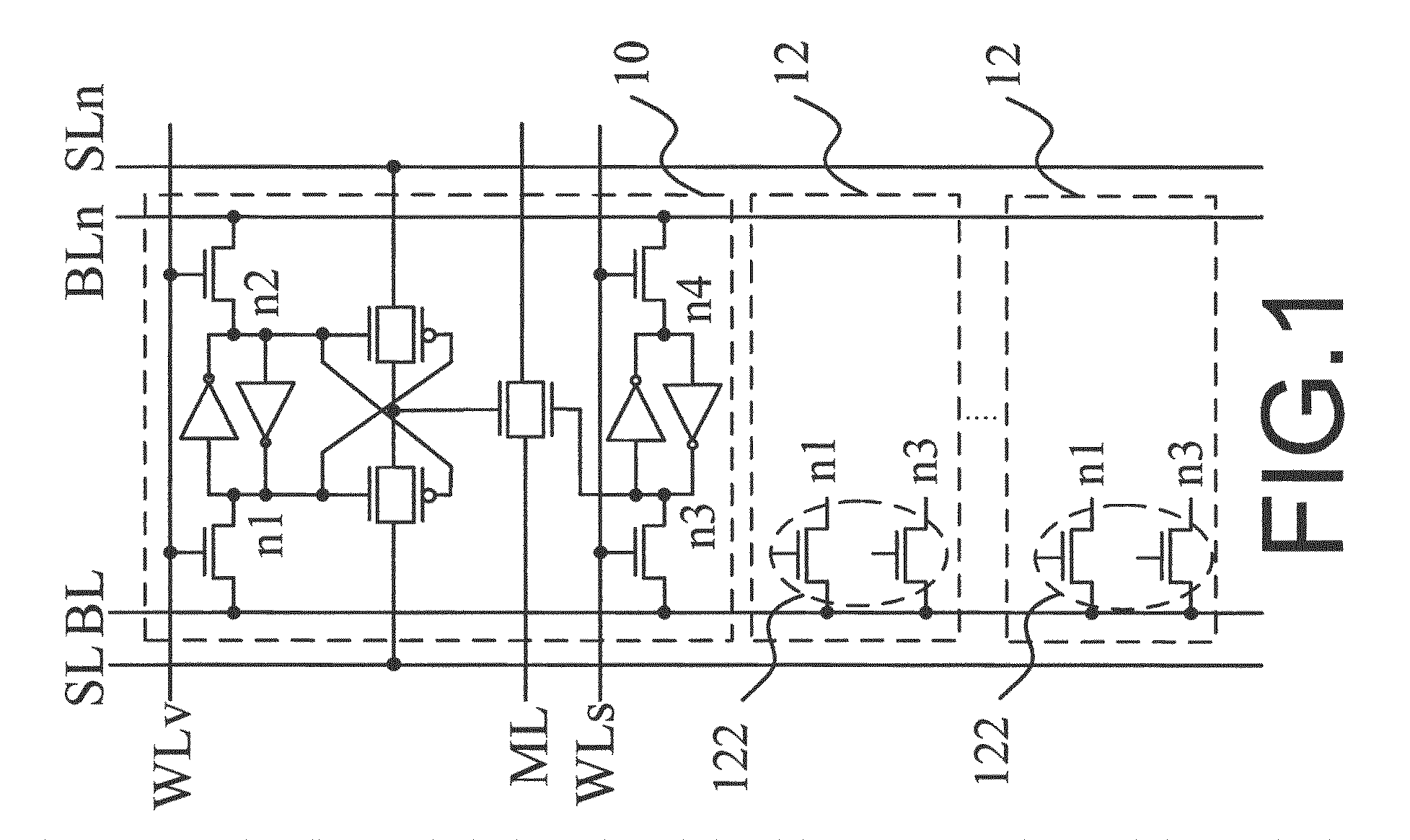
Thus, the static noise margin is decreased, and the external noise is more likely to affect the stability of the stored data.
Once the noise exceeds the allowance, the stored data is damaged.
The influence of current leakage is another problem.
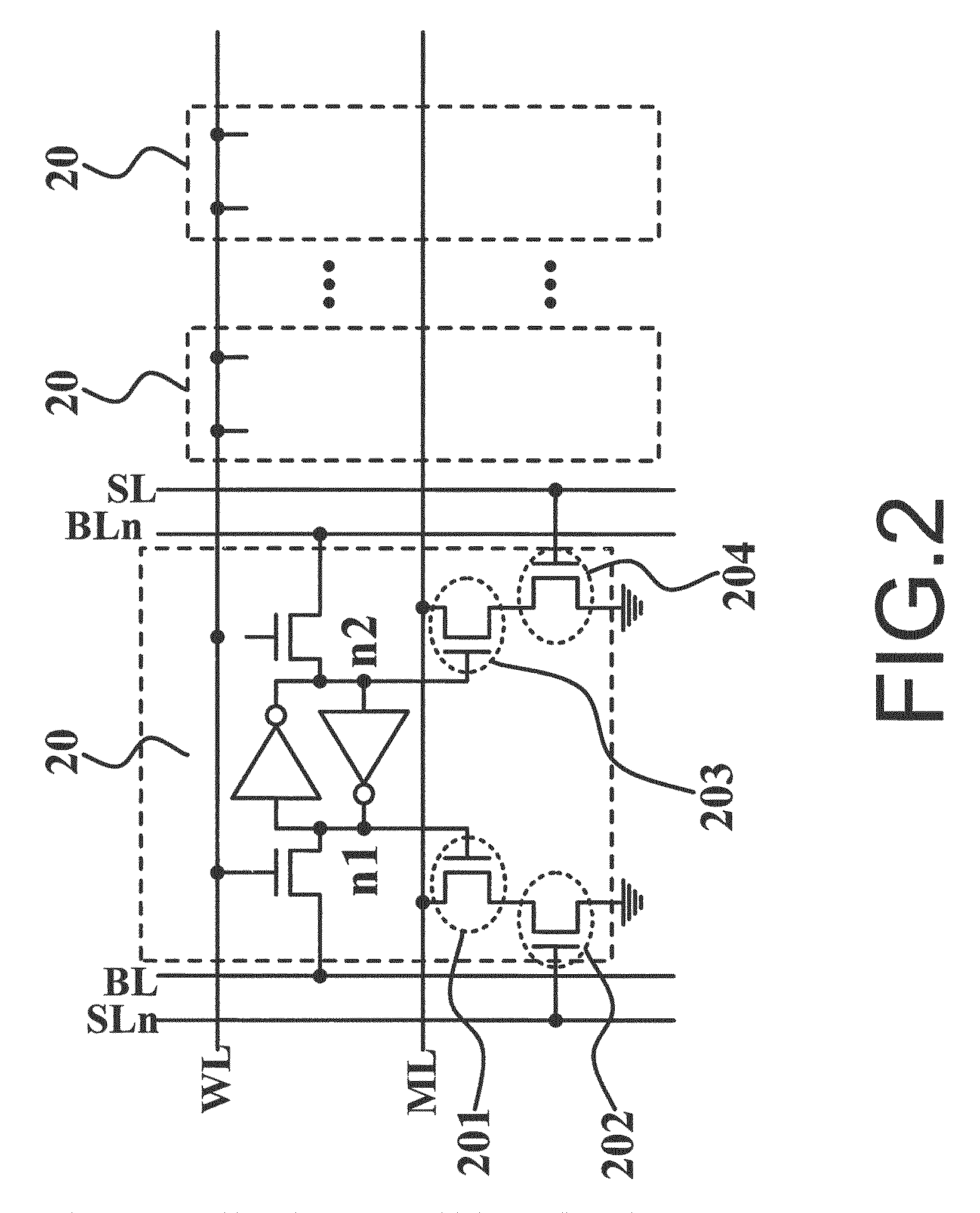
When executing a reading activity at a low voltage, the memory cell 20 also has the problems of static noise margin and bit-line current leakage.
The circuit further has a problem that the match line ML is affected by leakage current.

Method used


Image

  • Read and match circuit for low-voltage content addressable memory
  • Read and match circuit for low-voltage content addressable memory
  • Read and match circuit for low-voltage content addressable memory

Examples


first embodiment

[0041]The NAND-type CAM cell can apply to the NAND-type match-line circuit and the AND-type match-line circuit. Refer to FIG. 13 for the application of the present invention. The NAND-type CAM cell 180 may be the NAND-type ternary CAM cell 31 in FIG. 3 or the binary NAND-type CAM cell in FIG. 11, and the match output circuit 1802 may be the match output circuit 606 in FIG. 7 or the match output circuit 1404 in FIG. 11. In a pre-charge state, the control line clk of the match-line pre-charge circuit 70 has a logic value 0, and Node n1 has a logic value 1, and Node n2 has a logic value 0. Whether the bit matches the searched value determines whether the transistor of the match output circuit 1802 turns on or disconnects. When the bit matches the searched value, the corresponding transistor turns on. When the bit mismatches the searched value, the corresponding transistor disconnects. In an evaluate state, the control line clk has a logic value 1. If all the bits in the match output ci...

second embodiment

[0042]The NOR-type CAM cell can apply to the NOR-type match-line circuit. Refer to FIG. 14 for the application of the present invention. The NOR-type CAM cell 190 may be the NOR-type ternary CAM cell 32 in FIG. 3 or the binary NOR-type CAM cell in FIG. 12, and the match output circuit 1902 may be the match output circuit 1106 in FIG. 9 or the match output circuit 1704 in FIG. 12. In a pre-charge state, the control line clk has a logic value 0, and Node n1 has a logic value 1. Whether the bit matches the searched value determines whether the transistor of the match output circuit 1902 turns on or disconnects. If the bit matches the searched value, the corresponding transistor of the match output circuit 1902 disconnects. If the bit mismatches the searched value, the corresponding transistor of the match output circuit 1902 turns on. In an evaluate state, the control line clk has a logic value 1, and Node n2 has a logic value 0. If all the bits in the match output circuit 1902 match t...

third embodiment

[0043]The NAND-type CAM cell and the NOR-type CAM cell may also be used in an identical match line simultaneously. Refer to FIG. 15 for the application of the present invention. The NAND-type CAM cell group 200 may be the same as that shown in FIG. 13, and the NOR-type CAM cell group 210 may be the same as that shown in FIG. 14. In a pre-charge state, the control line clk has a logic value 0; Node n1 has a logic value 1; Node n2 has a logic value 0; Node n3 has a logic value 1; Node n5 has a logic value 0. The NAND-type CAM cell group 200 and the NOR-type CAM cell group 210 simultaneously undertake bit matching activities. In an evaluate state, the control line clk has a logic value 1. If all the bits of the NAND-type CAM cell 200 hit the searched values, Node n2 is shifted to a logic state of 1. If the bits of the NAND-type CAM cell 200 do not all hit the searched values, Node n2 is maintained at a logic state of 0, and Node n5 also has a logic value 0. When Node n1 is shifted to a...


PUM


Abstract

A read, write, and match circuit for a low-voltage content addressable memory. A write circuit inputs signals for storing data in the memory cells, a read circuit retrieves the stored data from the memory cells, and a match circuit compares the data stored in the memory cell with the data searched by the match circuit. The circuits for writing, reading and matching are separated from each other and exempt from mutual interference.

Description

BACKGROUND OF THE INVENTION[0001]1. Field of the Invention[0002]The present invention relates to a logic circuit, particularly to a read and match circuit for a low-voltage content addressable memory.[0003]2. Description of the Related Art[0004]A content addressable memory (CAM) not only stores data but also compares data. Therefore, a CAM cell not only has circuits for reading and writing data but also has transistors for matching data, wherein the data in the memory array is simultaneously compared with the searched data input externally. The mass parallel comparison operation has an advantage of high speed and a disadvantage of high power consumption.[0005]Refer to FIG. 1 for the architecture of bit lines in a conventional technology. Suppose that Node n1 is at a logic state of 1 and Node n2 is at a logic state of 0 in the memory cell 10, and suppose that the word line WLv is at a logic state of 1 and the bit lines BL and BLn are at a logic state of 1 in a reading activity. The p...

Claims


Application Information

Patent Timeline
Patent Type & Authority Patents(United States)
IPC IPC(8): G11C15/00
CPCG11C7/02G11C15/04
Inventor WANG, JINN-SHYANCHEN, TAI-AN
Owner NATIONAL CHUNG CHENG UNIV
Learn More