
Semiconductor device

a technology of semiconductor devices and dielectric devices, applied in the direction of logic circuit coupling/interface arrangements, pulse techniques, instruments, etc., can solve the problems of noise generation in input and output signals, difficulty in performing highly accurate impedance adjustment, and change in dq driver code through

Active Publication Date: 2011-09-13
LONGITUDE LICENSING LTD
View PDF3 Cites 17 Cited by
  • Summary
  • Abstract
  • Description
  • Claims
  • Application Information

AI Technical Summary

Benefits of technology

This approach allows for precise impedance adjustments without disrupting active operations, reducing noise in input / output signals and enabling efficient data transfer by separating calibration from operational periods.

Problems solved by technology

Therefore, it is difficult to perform the highly accurate impedance adjustment.
Therefore, there was a problem in that when a READ or WRITE command is input from an external semiconductor device, for example a memory controller, during the calibration period, a change in DQ driver code may occur through the whole of a period of time when the input / output circuit is activated, whereby noise may be generated in an input and output signal of the input / output circuit.

Method used


Image

  • Semiconductor device
  • Semiconductor device
  • Semiconductor device

Examples


first embodiment

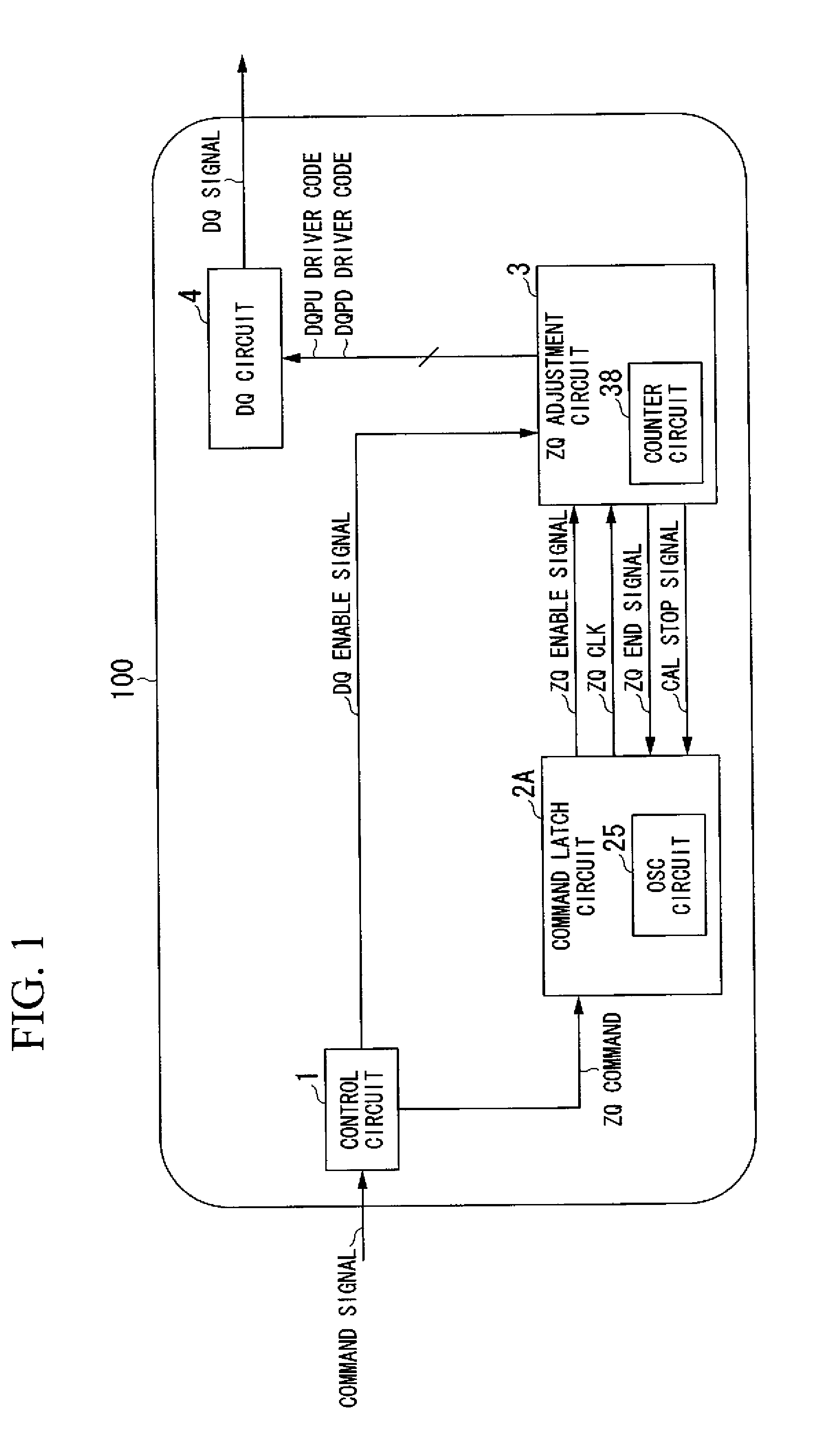
[0047]FIG. 1 is a block diagram of a semiconductor device 100 according to an embodiment of the invention.

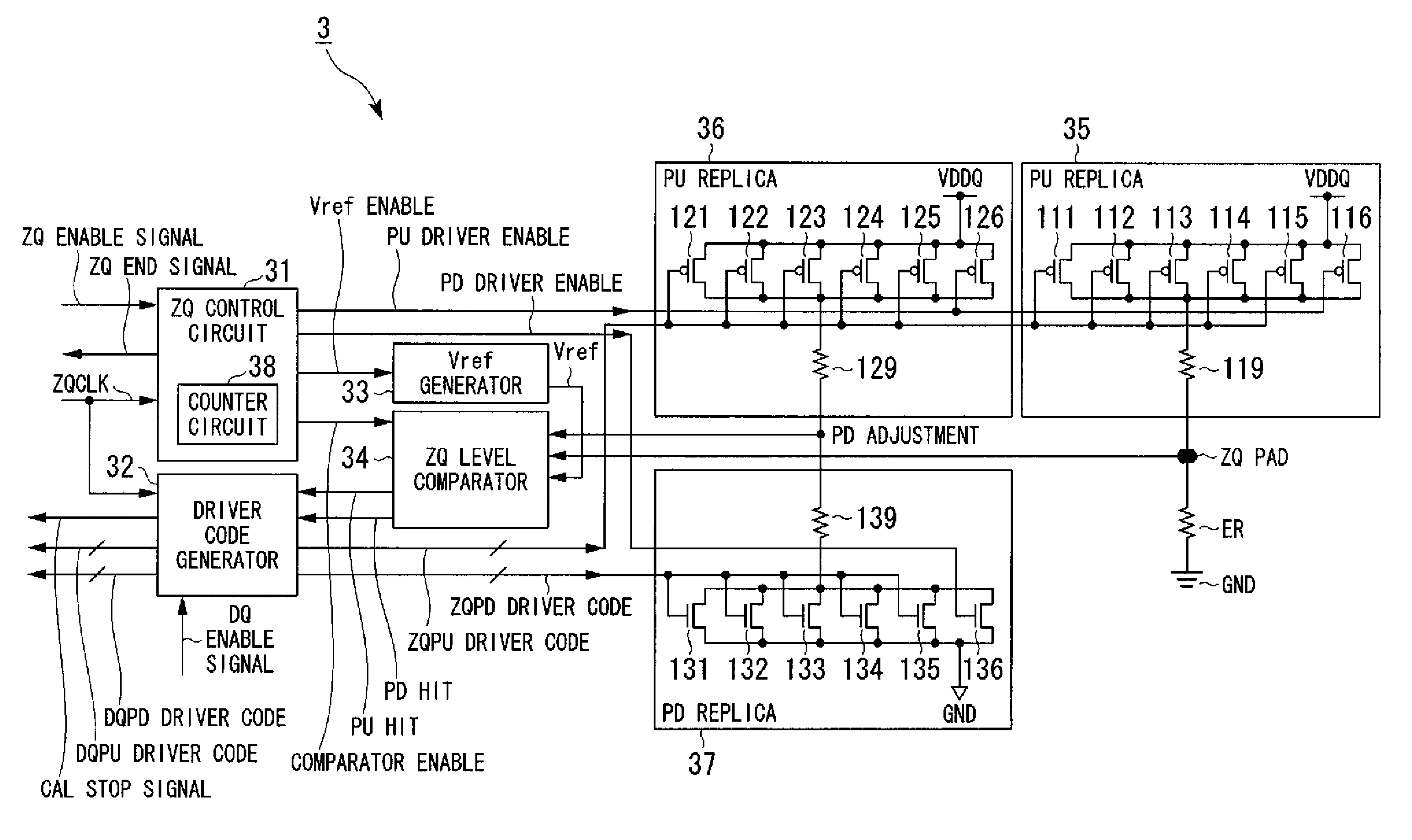
[0048]In FIG. 1, the semiconductor device 100 includes a control circuit 1, a command latch circuit 2A, a ZQ calibration circuit 3, and a DQ circuit 4.

[0049]In this embodiment, the semiconductor device 100 performs an impedance adjustment (ZQ calibration) between an external resistor element ER connected to a ZQ terminal and an internal replica buffer upon receiving a calibration command. The DQ circuit 4 receives and reflects therein this calibration result (DQ driver code) and changes the size of a driver of an output buffer. The control circuit 1 generates a signal (DQ Enable signal) indicating that an input / output circuit (the DQ circuit 4) is activated, upon receiving a READ or WRITE command. The ZQ calibration circuit 3 holds the DQ driver code in a latch circuit during an activation period of the input / output circuit (the DQ circuit4). The ZQ calibration circuit 3 supplie...

second embodiment

[0156]A second embodiment of the invention will be described.

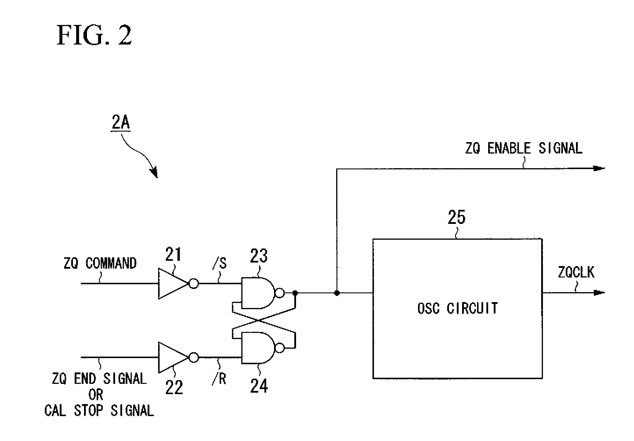
[0157]In this embodiment, a case where the driver code generation circuit 32 has a configuration shown in the block diagram of FIG. 4B will be described.

[0158]In FIG. 4B, the driver code generation circuit 32 includes a code update circuit 46, a latch circuit 47, an inverter circuit 48, a NAND circuit 49, and an inverter circuit 50.

[0159]The code update circuit 46 may have the same configuration as the code update circuit 41 described above. The code update circuit 46 is configured to output the ZQ driver code which is 10-bit data, i.e., the sum of the ZQPU driver code and the ZQPD driver code, to the replica circuit of the ZQ calibration circuit 3. The code update circuit 46 supplies the DQ driver code b1 to the latch circuit 47 upon receiving both the PU Hit and PD Hit signals.

[0160]The inverter circuit 48 is a NOT circuit which inverts the logic level of the DQ Enable signal. The NAND circuit 49 is a NOT circuit with th...


PUM


Abstract

A device includes a first circuit and an adjustment circuit. The adjustment circuit performs an adjustment on impedance of the first circuit. The adjustment circuit discontinues the adjustment on impedance while the first circuit is in an activated state.

Description

BACKGROUND OF THE INVENTION[0001]1. Field of the Invention[0002]The present invention generally relates to a semiconductor device. More specifically, the present invention relates to a semiconductor device such as DRAM (Dynamic Random Access Memory) which has a calibration circuit that adjusts impedance of an output buffer included in an output circuit.[0003]Priority is claimed on Japanese Patent Application No. 2009-023657, filed Feb. 4, 2009, the content of which is incorporated herein by reference.[0004]2. Description of the Related Art[0005]In a semiconductor device such as a DRAM, in order to execute high-speed data transfer, it is necessary to achieve an impedance adjustment in a transfer system to suppress distortion in data transfer waveforms due to reflection.[0006]Such an impedance adjustment is performed by adjusting the impedance of an output buffer circuit with a calibration circuit.[0007]Japanese Unexamined Patent Application, First Publication, No. JP-A-2008-048361 di...

Claims


Application Information

Patent Timeline
Patent Type & Authority Patents(United States)
IPC IPC(8): H03K19/003H03K17/16
CPCG11C7/1051G11C7/1057G11C11/4096H03K19/0005G11C2207/2254
Inventor KAIWA, NAKABAIKEDA, YUTAKA
Owner LONGITUDE LICENSING LTD
Learn More