Methods of manufacturing variable resistance non-volatile memory devices including a uniformly narrow contact layer

a non-volatile memory and contact layer technology, applied in semiconductor devices, digital storage, instruments, etc., can solve problems such as data loss of volatile memory devices, and achieve the effect of improving electrical characteristics of phase changeable memory devices and uniform cross-section and heigh

Inactive Publication Date: 2011-10-18
SAMSUNG ELECTRONICS CO LTD
View PDF17 Cites 10 Cited by
  • Summary
  • Abstract
  • Description
  • Claims
  • Application Information

AI Technical Summary

Benefits of technology

[0028]According to some embodiments of the present invention, after the preliminary first electrode including polysilicon is formed, both side portions of the preliminary first electrode are partially etched so that the first electrode having a relatively uniform cross-section and height may be formed. In addition, the spacer may be additionally formed on the sidewalls of the first electrode having a relatively uniform size. Therefore, the first electrode and the diode may make contact with each other satisfactorily regardless of a subsequent polishing process. In addition current may be uniformly provided to the phase changeable material layer pattern through the first electrode having the relatively uniform size so that electrical characteristics of the phase changeable memory device may be improved.

Problems solved by technology

On the other hand, the volatile memory devices may lose their data when power is off.

Method used


Image

  • Methods of manufacturing variable resistance non-volatile memory devices including a uniformly narrow contact layer
  • Methods of manufacturing variable resistance non-volatile memory devices including a uniformly narrow contact layer
  • Methods of manufacturing variable resistance non-volatile memory devices including a uniformly narrow contact layer

Examples


Embodiment Construction

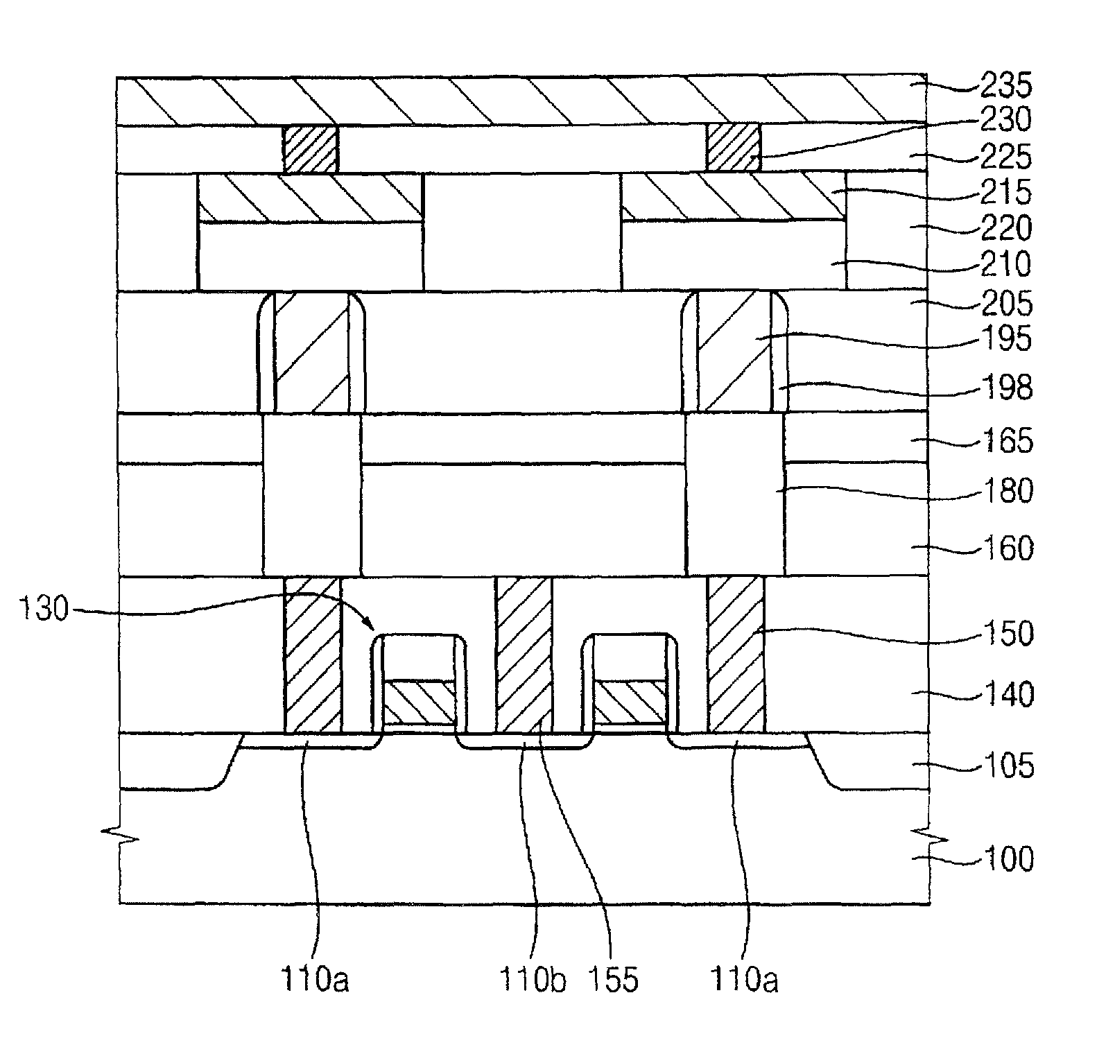
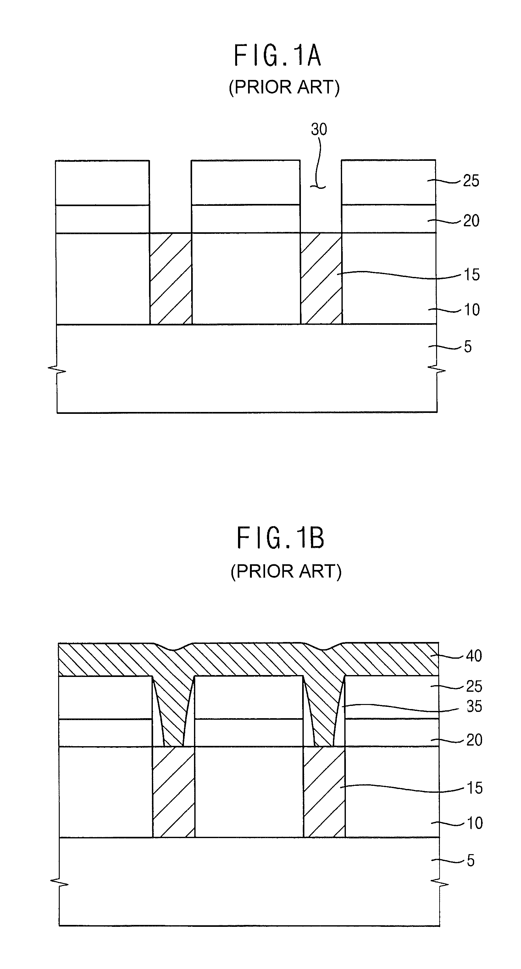
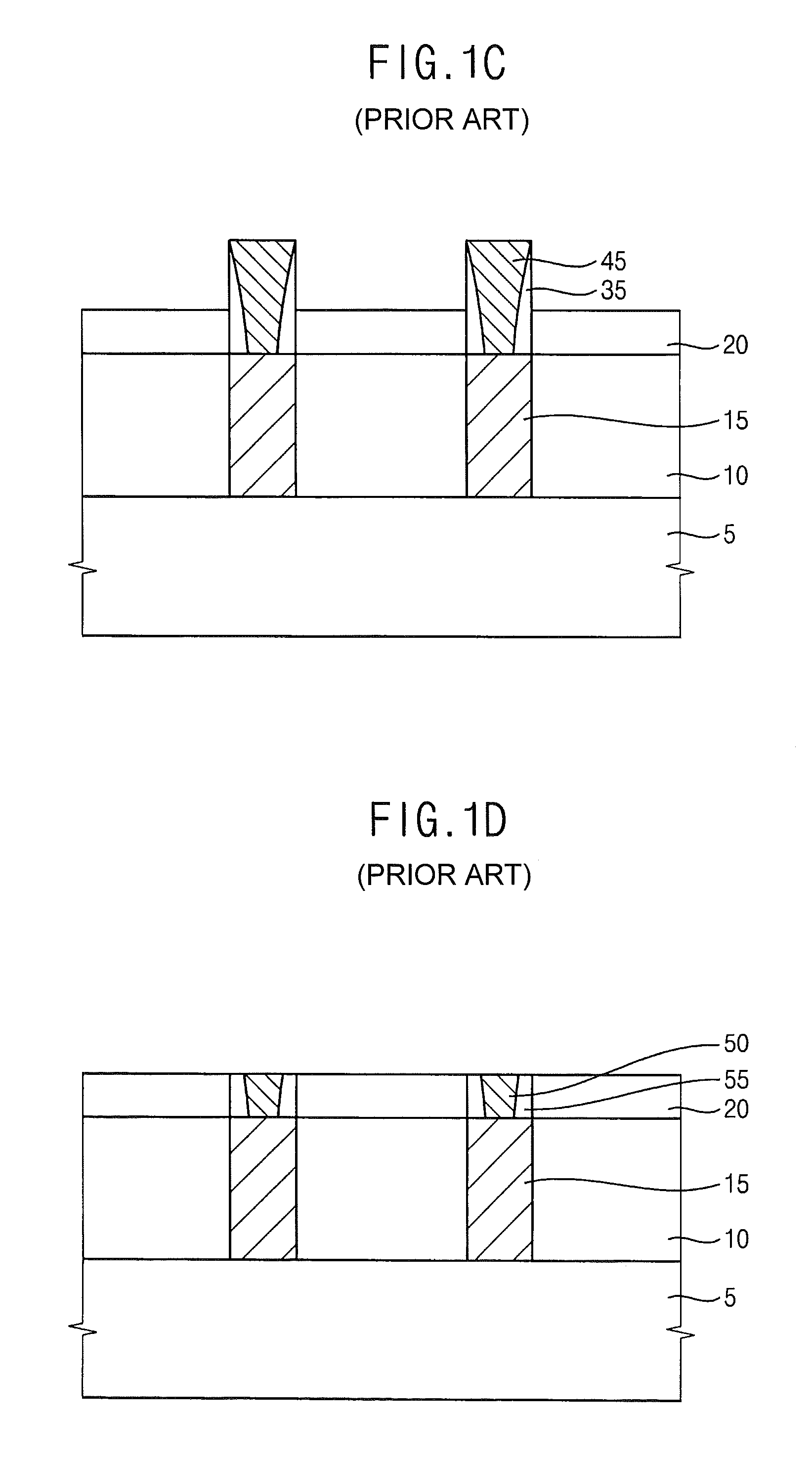
[0033]The present invention will now be described more fully hereinafter with reference to the accompanying drawings, in which exemplary embodiments of the invention are illustrated. The invention may, however, be embodied in different forms and should not be construed as limited to the embodiments set fourth herein. Rather, these embodiments are provided so that this disclosure will be thorough and complete, and will fully convey the scope of the invention to those skilled in the art.

[0034]It will be understood that when an element or layer is referred to as being “on,”“connected to” and / or “coupled to” another element or layer, the element or layer may be directly on, connected and / or coupled to the other element or layer, or intervening elements or layers may be present. In contrast, when an element is referred to as being “directly on,”“directly connected to” and / or “directly coupled to” another element or layer, no intervening elements or layers are present. As used herein, the...


PUM


Abstract

A phase changeable memory device is manufactured by forming at least one insulating layer on a substrate. A preliminary first electrode is formed on the insulating layer. The preliminary first electrode is partially etched to form a first electrode electrically connected to the substrate. After the preliminary first electrode is formed, both sidewalls of the preliminary first electrode are partially etched isotropically to form a first electrode having a uniform width and height. A phase changeable material layer pattern and a second electrode are subsequently formed on the first electrode. Related devices also are described.

Description

CROSS-REFERENCE TO RELATED APPLICATION[0001]This application claims the benefit under 35 USC §119 of Korean Patent Application No. 10-2006-0072469, filed on Aug. 1, 2006, the disclosure of which is hereby incorporated herein by reference in its entirety as if set forth fully herein.FIELD OF THE INVENTION[0002]The present invention relates to non-volatile memory devices and manufacturing methods therefor; and more specifically to variable resistance non-volatile memory devices and manufacturing methods therefor.BACKGROUND OF THE INVENTION[0003]Integrated circuit (semiconductor) memory devices include dynamic random access memory (DRAM) devices, static random access memory (SRAM) devices, flash memory devices, etc. In addition, the memory devices may be classified as volatile memory devices or non-volatile memory devices. The non-volatile memory devices may retain their data even though power is off. On the other hand, the volatile memory devices may lose their data when power is off....

Claims


Application Information

Patent Timeline
Patent Type & Authority Patents(United States)
IPC IPC(8): H01L21/62
CPCH01L27/2409H01L27/2436H01L45/06H01L45/1233H01L45/126H01L45/143H01L45/144H01L45/1675H10B63/20H10B63/30H10N70/231H10N70/826H10N70/8413H10N70/8825H10N70/8828H10N70/063G11C13/0004
Inventor MIN, CHUNG-KIKIM, TAE-EUNYOON, BYOUNG-MOON
Owner SAMSUNG ELECTRONICS CO LTD
Why Eureka
Try Eureka