Method and system for bonding 3D semiconductor devices

a semiconductor device and 3d technology, applied in the field of semiconductor device fabrication, can solve the problems of chemical residues and deleterious materials, and interfere with bonding, and achieve the effects of reducing oxidation of exposed conductive materials, better adhesion, and better bonding stability

Inactive Publication Date: 2011-11-01
TAIWAN SEMICON MFG CO LTD
View PDF10 Cites 5 Cited by
  • Summary
  • Abstract
  • Description
  • Claims
  • Application Information

AI Technical Summary

Benefits of technology

[0010]An advantage of preferred embodiments of the present invention is that oxidation of the exposed conductive material is reduced and undesirable moisture and chemical residue is largely or completely expelled. This generally provides for better adhesion and, as a result, better bonding stability.
[0011]A further advantage of a preferred embodiment of the present invention is that process Q-time is prolonged, easing time constraints otherwise present in the fabrication process without incurring significant additional cost.

Problems solved by technology

Unfortunately, when using vertical conductive structures to make connections between the components of one semiconductor device and those of another, problems in bonding may occur.
The processes used to prepare one chip for bonding with another, such as grinding and polishing, often leave behind chemical residue and deleterious material that interferes with the bonding process.
In addition, if too much time is allowed to elapse between preparation and bonding, oxidation or corrosion may degrade the quality of the exposed conductors.
Eliminating this delay (sometimes referred to as Queue-time, or simply Q-time), however, may impose addition costs or other undesirable consequences.

Method used


Image

  • Method and system for bonding 3D semiconductor devices
  • Method and system for bonding 3D semiconductor devices
  • Method and system for bonding 3D semiconductor devices

Examples


Embodiment Construction

[0021]The making and using of the presently preferred embodiments are discussed in detail below. It should be appreciated, however, that the present invention provides many applicable inventive concepts that can be embodied in a wide variety of specific contexts. The specific embodiments discussed are merely illustrative of specific ways to make and use the invention, and do not limit the scope of the invention.

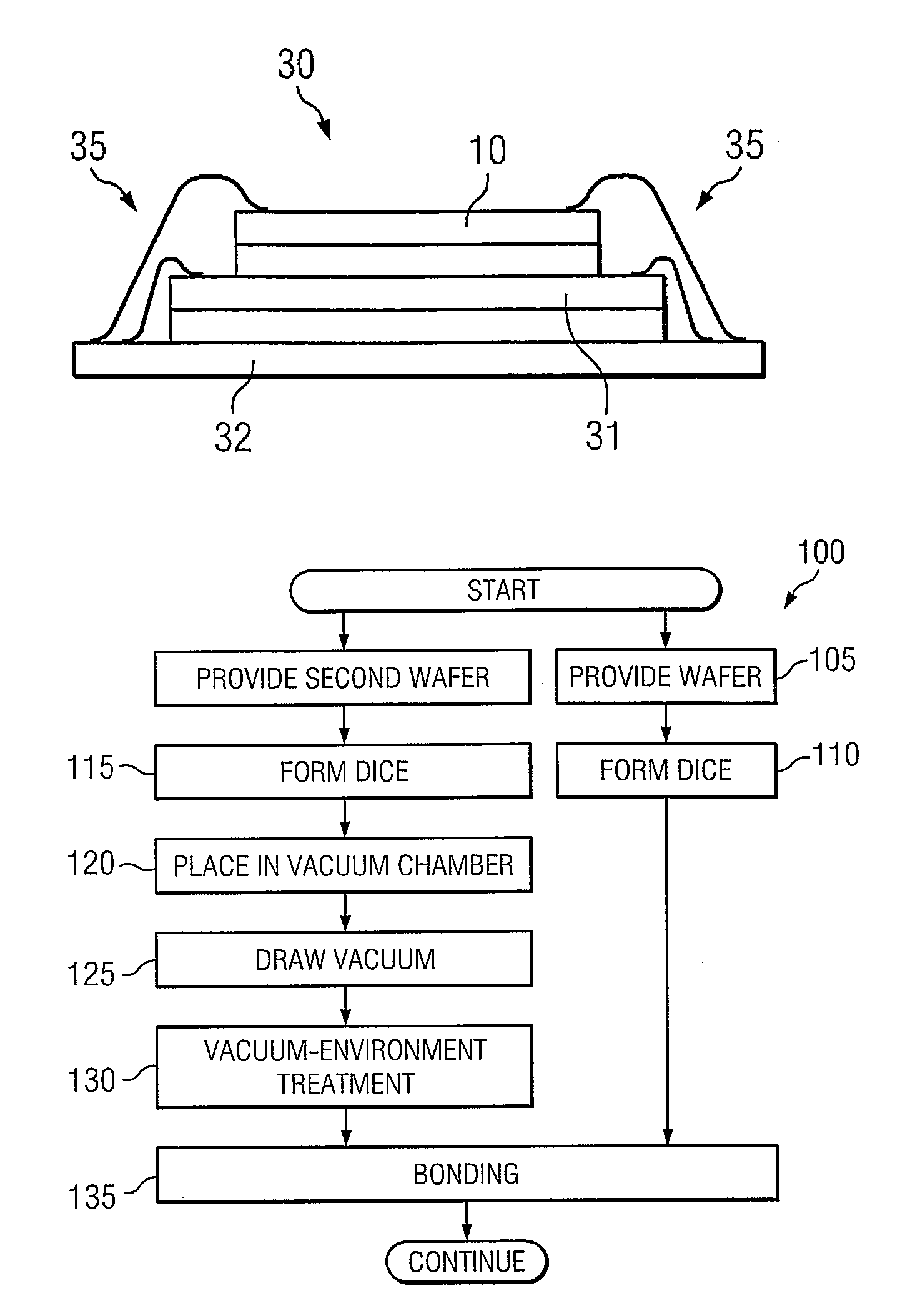
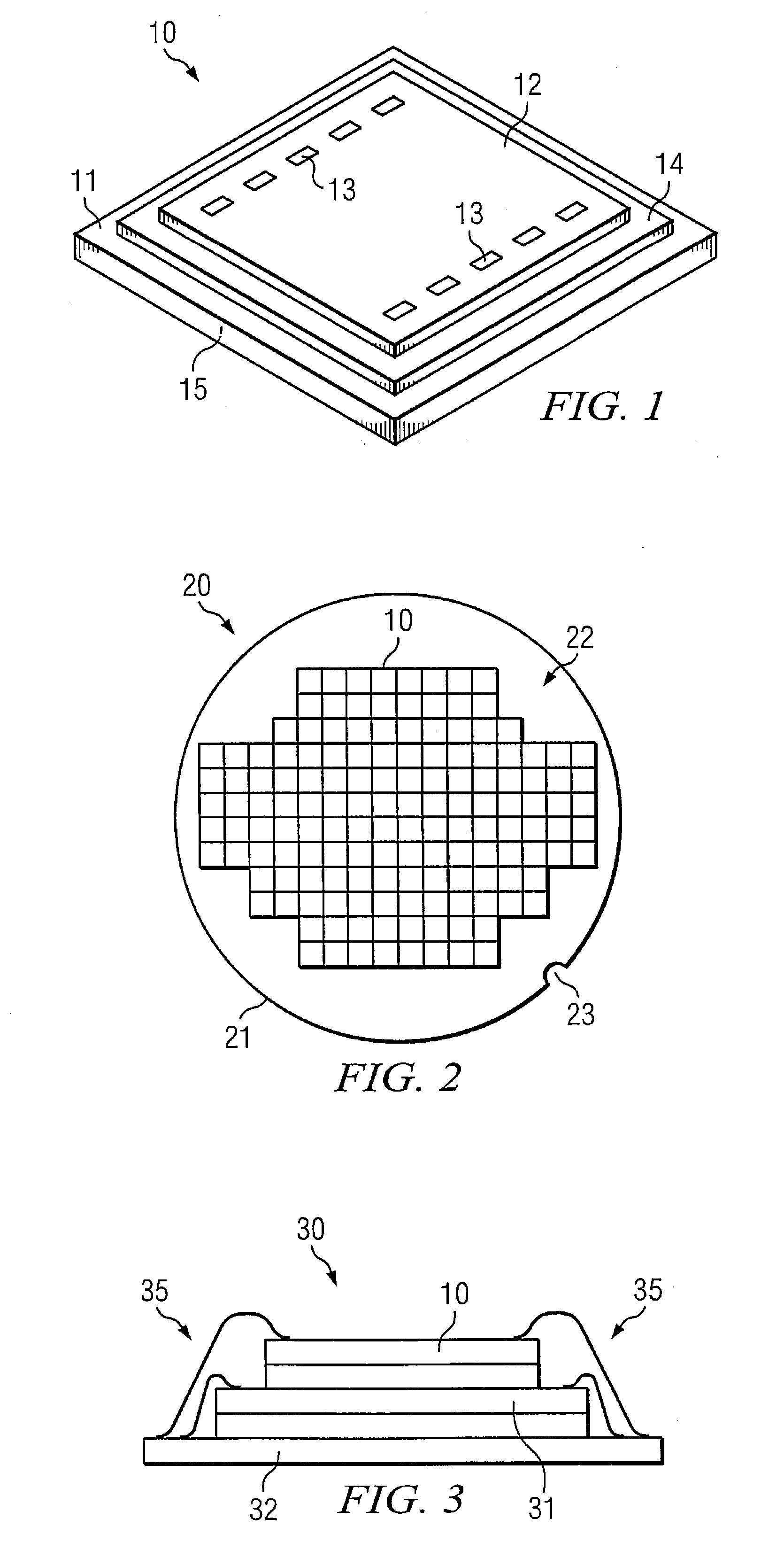
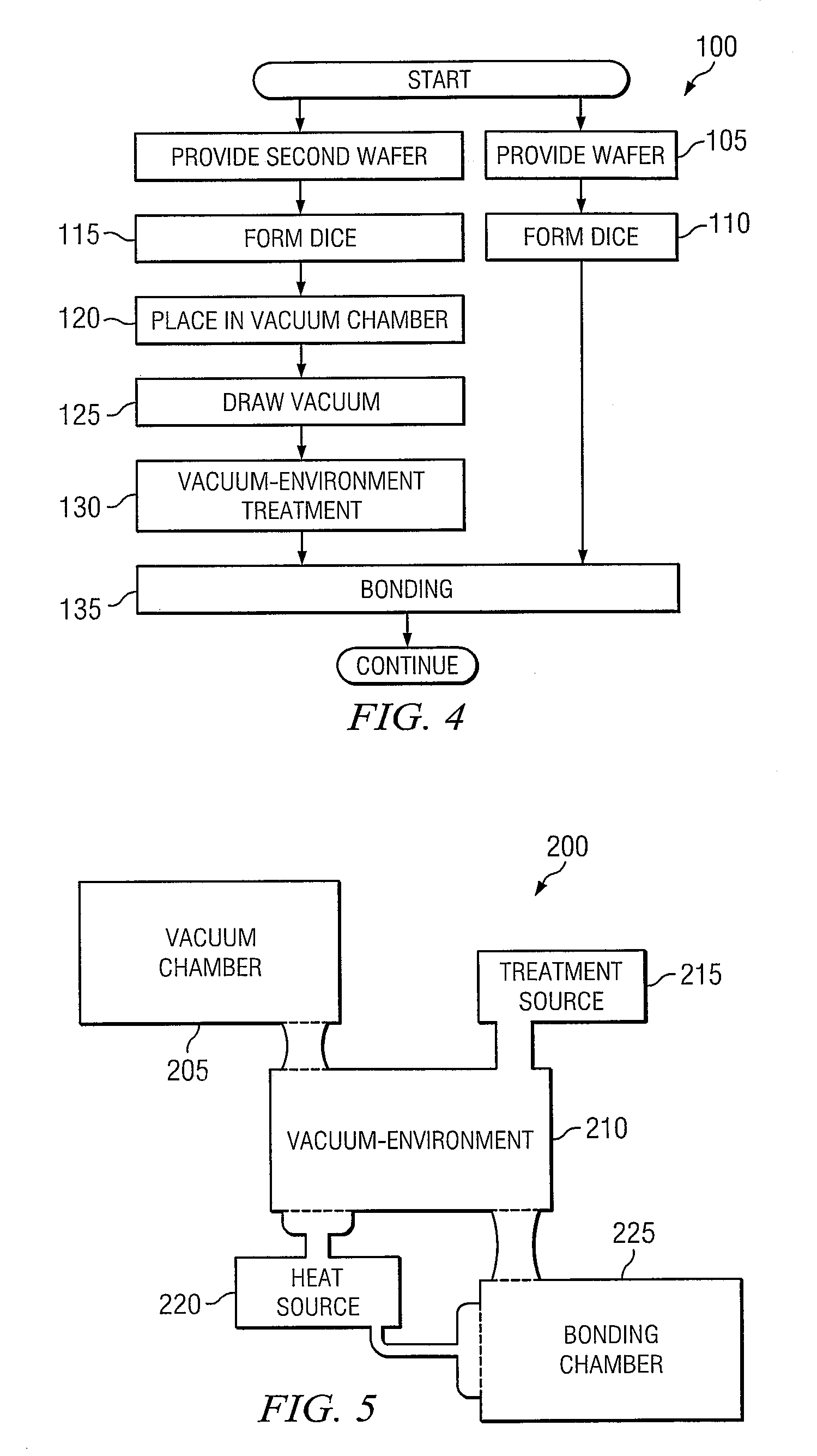
[0022]The present invention will be described with respect to preferred embodiments in a specific context, namely a 3D (three-dimensional) SIC (stacked integrated circuit) semiconductor device. The invention may also be applied, however, to other semiconductor devices as well. As mentioned above, the present invention is directed to a method and system for providing longer Q-times at certain stages of the chip manufacturing process, and for reducing the risk of bonding failure by reducing the amount of moisture and residual chemicals remaining on the bonding surface after pre...


PUM


Abstract

A method and system and for fabricating 3D (three-dimensional) SIC (stacked integrated chip) semiconductor devices. The system includes a vacuum chamber, a vacuum-environment treatment chamber, and a bonding chamber, though in some embodiments the same physical enclosure may serve more than one of these functions. A vacuum-environment treatment source in communication with the vacuum-environment treatment chamber provides a selected one or more of a hydrogen (H2)-based thermal anneal, an H2-based plasma treatment, or an ammonia (NH3)-based plasma treatment. In another embodiment, a method includes placing a semiconductor chip in a vacuum environment, performing a selected vacuum-environment treatment, and bonding the chip to a base wafer. A plurality of chips formed as dice on a semiconductor wafer may, of course, be simultaneously treated and bonded in this way as well, either before or after dicing.

Description

TECHNICAL FIELD[0001]The present invention relates generally to the fabrication of semiconductor devices, and related more particularly to a system and method for bonding together the separate chips in a 3D (three-dimensional) semiconductor device such as a 3D-SIC (stacked integrated circuit) SIP (system in package) device.BACKGROUND[0002]Modern electronic appliances are frequently manufactured using one or more packaged semiconductor devices, which are sometimes called chips, each enclosed in a familiar black plastic package or in some other type of protective enclosure. Each chip performs a specific function associated with the operation of electronic appliance, and is mounted on one or more printed wired boards (PWBs) that provide for mechanical support and for electrical connections between the various chips. The PWBs and one or more input and output devices such as keyboards or LCD screens are then secured in some type of housing. Examples of modern electronic appliances includ...

Claims


Application Information

Patent Timeline
Patent Type & Authority Patents(United States)
IPC IPC(8): H01L21/00
CPCH01L21/6835H01L21/6836H01L21/76898H01L24/95H01L24/97H01L25/0657H01L25/50H01L2221/68327H01L2221/68354H01L2224/16H01L2224/32145H01L2224/48227H01L2225/06513H01L2225/06541H01L2924/01015H01L2924/01029H01L2924/01032H01L2924/01033H01L2924/14H01L2224/48091H01L2224/48472H01L2924/00014H01L2224/73265H01L2924/01006H01L2924/00H01L2224/97H01L2224/05553H01L21/762H01L21/50
Inventor LIU, CHUNG-SHIYU, CHEN-HUAMII, YUH-JIERSUN, YUAN-CHEN
Owner TAIWAN SEMICON MFG CO LTD
Why Eureka
Try Eureka