3D silicon-silicon die stack structure and method for fine pitch interconnection and vertical heat transport

a technology of silicon-silicon dies and stack structures, applied in the direction of individual semiconductor device testing, semiconductor/solid-state device testing/measurement, instruments, etc., can solve the problems of excessive power required to drive data to and from the chip to the memory, increase system performance, power efficiency and cost, etc., to achieve efficient circuit dense regions, reduce power distribution costs, and large current carrying capacity

Inactive Publication Date: 2011-11-01
GLOBALFOUNDRIES INC
View PDF20 Cites 48 Cited by
  • Summary
  • Abstract
  • Description
  • Claims
  • Application Information

AI Technical Summary

Benefits of technology

[0014]The thermal paths can utilize high thermal conductive materials, which may also be electrically conductive, such as solder in SSIs, copper used in wiring and TSVs, or simply adding thermal interconnections for improved heat transfer and / or mechanical integrity. The thermal paths can also utilize materials having high thermal conductivity but which are electrically insulating, such as BeO, SiC, carbon nanotubes, etc. Thus, to aide in removing heat from a die stack, thermal vias can be added to an ILD (inter-layer-dielectric), and underfills with improved thermal conductivity can be added between silicon strata levels and between other interconnections, such as solder interconnections, Cu—Cu and other electrical connections. The area of a conductor between silicon strata levels can be increased. Thus, the use of thermal TSVs and SSIs can aide in heat removal from a die stack, and the use of a larger SSI area also increases heat removal.
[0016]The proper choice of materials for interconnection can help avoid soft errors due to subatomic or cosmic particles that can cause errors in the resulting circuits. The use of low alpha solders such as alloys of AuSn, In, Sn, SnCu, In—Ni—Cu, SnAg or other alloys can service these interconnections. Large blocks of solder are used for thermal interconnection along with small interconnections of solder microbumps for signals and small or intermediate size diameter bumps for power. Bumps can be taylored for electrical, thermal, power and mechanical integrity. Areas over macros can have mechanical / thermal pads or an array of bumps, or other shapes, and the option of thermal vias in some or all of the BEOL and FEOL where it aids thermal conduction and fits an overall design. Adhesive underfill or no-flow underfills and / or combinations with seal bands can aide in mechanical integrity and corrosion protection of interconnections.
[0017]Ball-limiting metallurgy (BLM) is used for each silicon layer to provide a grid of power feed throughs at one or more voltages to support power distribution from TSV dense regions to macro regions lacking TSV's. A dielectric can be provided over power and / or ground distribution wiring to create a micro connection area on one side of an SSI and the same for the other side to create a large current carrying capability without added fat wire layers, thus keeping costs down in power distribution while maintaining efficient circuit dense regions. This can be accomplished by interconnecting wiring connections to the pads connected to solder bumps to create a wiring distribution or mesh to provide a power grid o which can support the application voltage levels and system requirements.
[0031]According to a further aspect of the invention, the silicon interposer is larger in horizontal directions than said die stack, wherein said substrate has a different coefficient of thermal expansion than said die stack, and wherein stresses resulting from attaching said die stack to said substrate are reduced.
[0034]According to a another aspect of the invention, there is provided a silicon-silicon die stack structure comprising a substrate, a plurality of thin silicon die wafer layers disposed on said substrate with a high density of vertical through-silicon-vias (TSVs) through the wafer layers for electrical interconnectivity, a silicon-silicon interconnection between each wafer layer, said silicon-silicon interconnection including a plurality of metallic interconnection and thermal paths surrounded by an adhesive dielectric layer, wherein said silicon-silicon interconnections further include solder interconnections of various size to provide high density arrays of signals in vertical paths and areas for thermal transport and power feed through, and underfills with improved thermal conductivity between silicon strata levels and between other interconnections for improved mechanical integrity and corrosion protection of interconnections, wherein larger blocks of solder are used for thermal interconnection, intermediate size diameter blocks of solder are used for power transmission, and smaller blocks of solder are used for signal transmission.
[0040]According to a further aspect of the invention, the silicon interposer has a larger horizontal dimension than the silicon die wafers in the stack, wherein said substrate has a different coefficient of thermal expansion than said die stack, and wherein stresses resulting from attaching said die stack to said substrate are reduced.

Problems solved by technology

Three-dimensional integrated circuits present several issues regarding the increase of system performance, power efficiency and cost.
These issues can be addressed with a die stack, but this its own challenges.
Challenges regarding a die stack include delivering power to the die stack, removing heat from die stack, and operation defects due to exposure to atomic particles, sub-atomic particles or radiation.
For example, alpha particles from cosmic rays or emitted by the materials used in the die stack or module can impact circuit operation and can cause machine errors.
Traditional packaging lacks sufficient input / output (I / O) connections to and from the chip, and even if there were enough connections, the power required to drive data to and from the chip to memory and to drive the memory chips themselves would become excessive.
Another challenge is that of localized heat removal from a hot spot on a die or from any strata level within the thinned die stack to a heat spreader, heat fins or a cold plate to remove excess heat from the die stack and / or module.
For a thinned die stack, the ability to remove heat from a hot spot and or a die stack can be more challenging.
Many existing structures do not achieve these elements in a vertical stack.

Method used


Image

  • 3D silicon-silicon die stack structure and method for fine pitch interconnection and vertical heat transport
  • 3D silicon-silicon die stack structure and method for fine pitch interconnection and vertical heat transport
  • 3D silicon-silicon die stack structure and method for fine pitch interconnection and vertical heat transport

Examples


Embodiment Construction

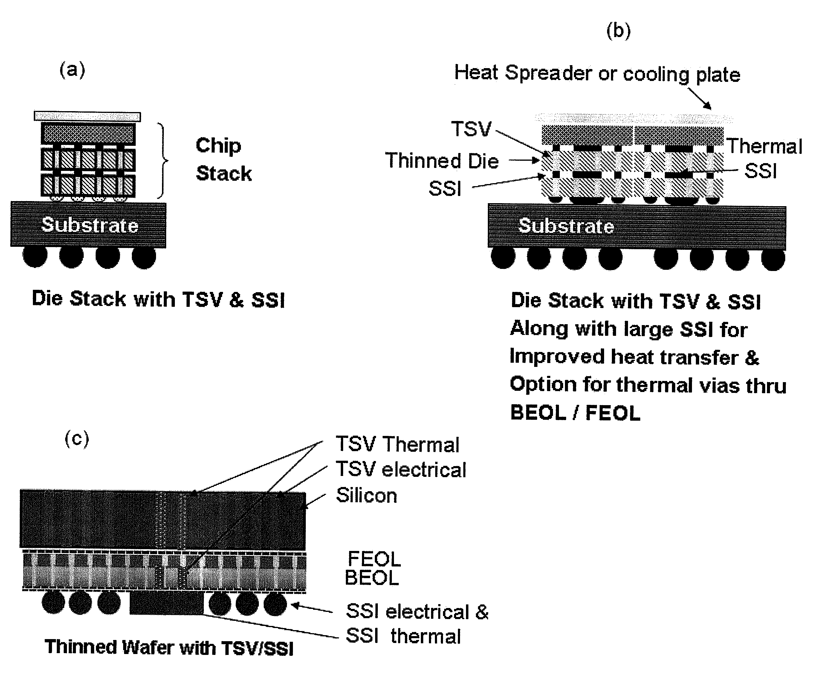
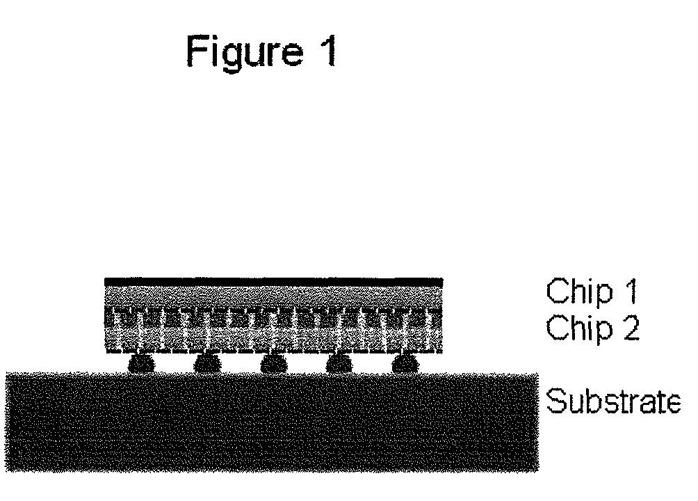
[0048]Exemplary embodiments of the invention as described herein generally include vertical stacked dies, dies on wafer, and wafer on wafer stacking. Accordingly, while the invention is susceptible to various modifications and alternative forms, specific embodiments thereof are shown by way of example in the drawings and will herein be described in detail. It should be understood, however, that there is no intent to limit the invention to the particular forms disclosed, but on the contrary, the invention is to cover all modifications, equivalents, and alternatives falling within the spirit and scope of the invention.

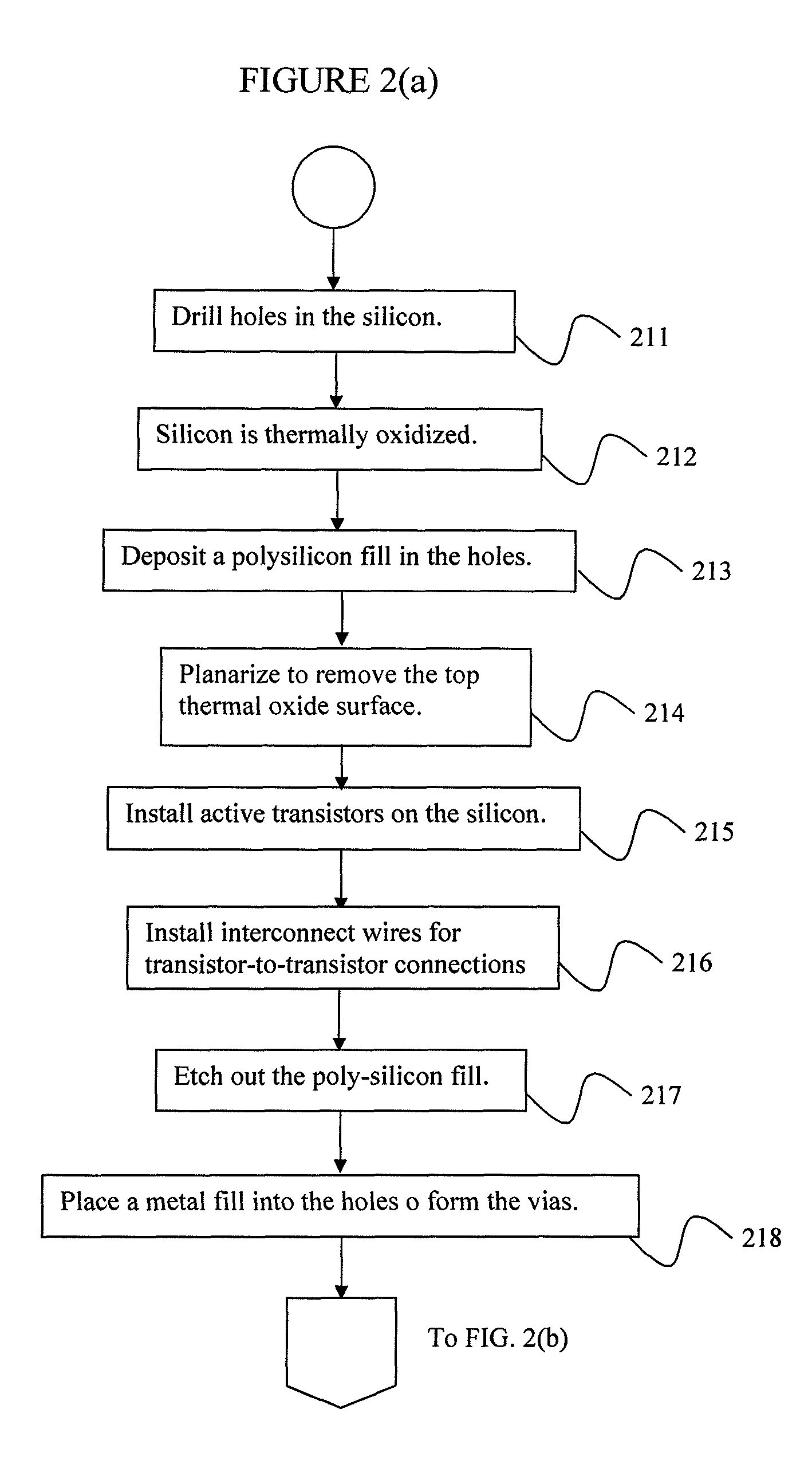
[0049]Traditional wafer fabrication involves putting down active circuits and wiring on one side of a silicon wafer. Typically, wafers used for 2-dimensional integrated circuits are from 430 microns thick down to 270 microns thick. The first portion of the integrated circuit fabrication, where the active transistors and local wiring to interconnect the transistors are pa...


PUM


Abstract

A method of fabricating a thin wafer die includes creating circuits and front-end-of-line wiring on a silicon wafer, drilling holes in a topside of the wafer, depositing an insulator on the drilled holes surface to provide a dielectric insulator, removing any excess surface deposition from the surface, putting a metal fill into the holes to form through-silicon-vias (TSV), creating back-end-of-line wiring and pads on the top surface for interconnection, thinning down the wafer to expose the insulator in from the TSVs to adapt the TSVs to be contacted from a backside of the wafer, depositing an insulating layer which contacts the TSV dielectric, thinning down the backside of the wafer, opening through the dielectric to expose the conductor of the TSV to provide a dielectric insulation about exposed backside silicon, and depositing ball limiting metallurgy pads and solder bumps on the backside of the wafer to form an integrated circuit.

Description

TECHNICAL FIELD[0001]This disclosure is directed to structures for use in three-dimensional integrated circuits, such as vertical stacked die, die on wafer, and wafer on wafer stacking.DISCUSSION OF THE RELATED ART[0002]Three-dimensional integrated circuits present several issues regarding the increase of system performance, power efficiency and cost. These issues can be addressed with a die stack, but this its own challenges. Challenges regarding a die stack include delivering power to the die stack, removing heat from die stack, and operation defects due to exposure to atomic particles, sub-atomic particles or radiation. For example, alpha particles from cosmic rays or emitted by the materials used in the die stack or module can impact circuit operation and can cause machine errors.[0003]Three-dimensional integrated circuits need an increased interconnection on and off the die stack to support a high level of communication across the die stack. For example, the need for increased ...

Claims


Application Information

Patent Timeline
Patent Type & Authority Patents(United States)
IPC IPC(8): H01L29/06
CPCH01L21/76898H01L22/20H01L2224/16145H01L2924/014H01L23/367
Inventor KNICKERBOCKER, JOHN U.
Owner GLOBALFOUNDRIES INC
Why Eureka
Try Eureka