Photoelectrochemical etching of P-type semiconductor heterostructures

a technology of p-type semiconductor and heterostructure, which is applied in the direction of semiconductor devices, electrical equipment, basic electric elements, etc., can solve the problems of difficult to achieve pec etching of p-type semiconductors, limited success in etching p-type layers, and elevated temperatures, so as to achieve smoothness or roughness, the effect of reducing the damage to the p-type semiconductor etched by p

Active Publication Date: 2011-11-08
RGT UNIV OF CALIFORNIA
View PDF12 Cites 3 Cited by
  • Summary
  • Abstract
  • Description
  • Claims
  • Application Information

AI Technical Summary

Benefits of technology

[0021]To overcome the limitations in the prior art described above, and to overcome other limitations that will become apparent upon reading and understanding the present specification, the present invention describes etching (e.g., wet etching, PEC etching) of p-type semiconductors simply and efficiently through the use of heterostructures.
[0024]The present invention allows for no substantial external bias to be applied to the p-type layer in order to etch the p-type layer. If an external bias is used, the internal electric field is typically stronger, thereby bringing holes to a surface of the p-type semiconductor layer faster, as compared to an electric field produced by an external bias applied to the device structure in order to etch the p-type layer. The internal electric field enables etching the p-type semiconductor layer at a rate comparable to an etch rate of an n-type semiconductor layer. The etch rate can be at least 2.8 nm per minute, using an external bias is less than 2 Volts, and the etching can produce a surface roughness of the p-type layer as smooth as a surface roughness of an n-type semiconductor layer etched under substantially similar conditions.
[0028]The present invention further discloses a heterostructure, comprising a p-type semiconductor having an etched surface, wherein damage to the p-type semiconductor etched by PEC is lower as compared to a p-type semiconductor etched by ion-assisted plasma etching or dry etching. For example, the PEC etching may not introduce any damage to the p-type semiconductor. The heterostructure may comprise an etched surface that is not a crystallographic plane of the p-type semiconductor, one or more anisotropic trenches in the p-type semiconductor, and / or a smoothness or roughness comparable to an etched surface of an n-type semiconductor.

Problems solved by technology

For GaN especially, PEC etching has been of great interest since there are very limited alternatives for room temperature wet etching.
Thus, PEC etching of p-type semiconductors has been difficult to achieve.
PEC etching is a well-established process used for n-type and unintentionally doped semiconductors, but it has had very limited success for etching p-type layers.
There have been limited reports of PEC etching of p-type semiconductors in the past, but they have generally required elevated temperatures, a substantial external bias on the system, or a complex experimental apparatus.
In addition, etch rates are generally very slow compared to n-type materials.
Either a very large bias is necessary or the etch rate is very slow.
They were able to obtain an etch rate of 2.8 nm / minute using this technique, but at the cost of increased roughness compared to similar etch conditions for n-type GaN.
However, this etch is very crystallographically selective, and also requires the use of quite elevated temperatures.
While feasible for fundamental studies of etching, this two-compartment geometry does not easily accommodate the practical etching of GaN devices.

Method used


Image

  • Photoelectrochemical etching of P-type semiconductor heterostructures
  • Photoelectrochemical etching of P-type semiconductor heterostructures
  • Photoelectrochemical etching of P-type semiconductor heterostructures

Examples


Embodiment Construction

[0039]In the following description of the preferred embodiment, reference is made to the accompanying drawings which form a part hereof, and in which is shown by way of illustration a specific embodiment in which the invention may be practiced. It is to be understood that other embodiments may be utilized and structural changes may be made without departing from the scope of the present invention.

Overview

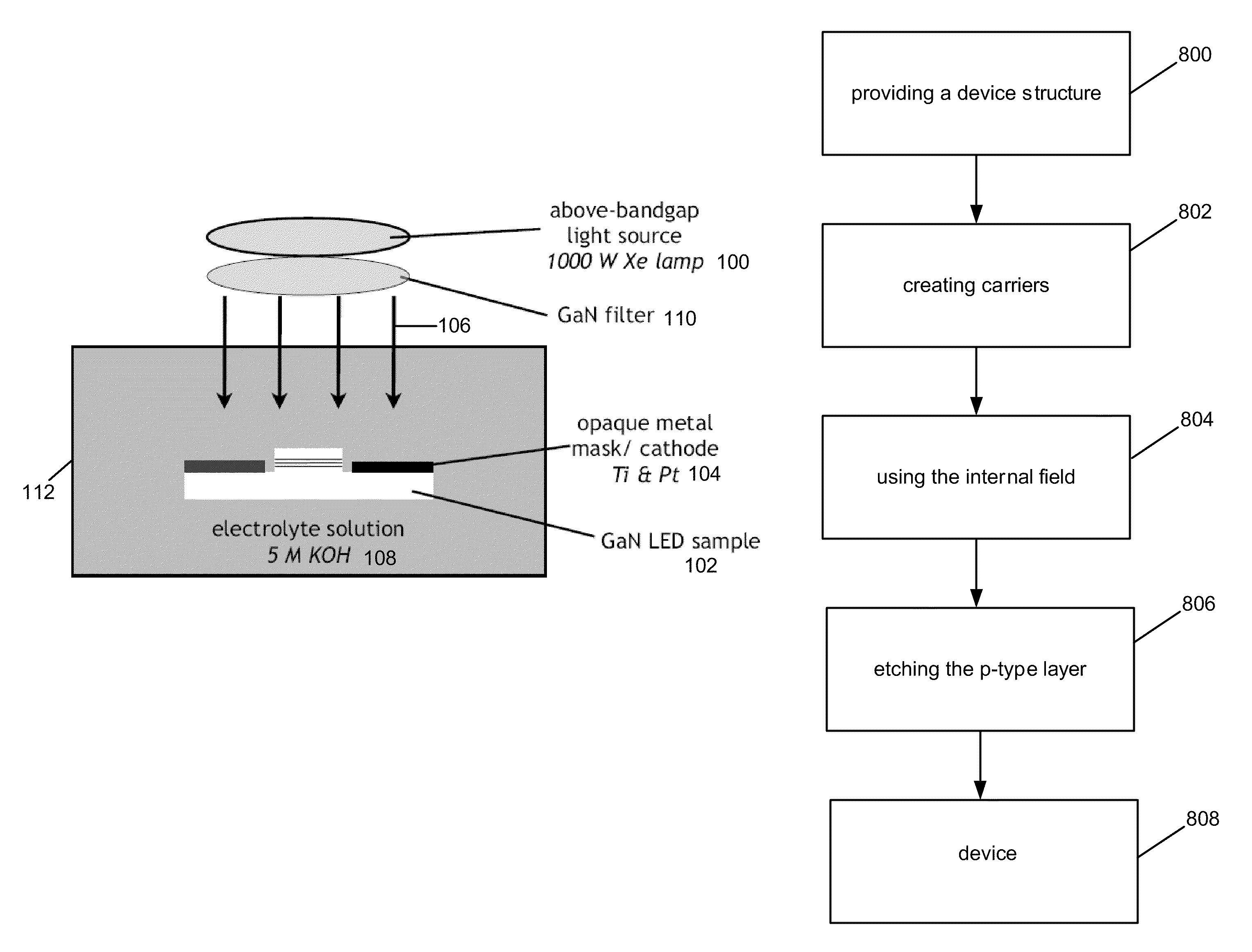
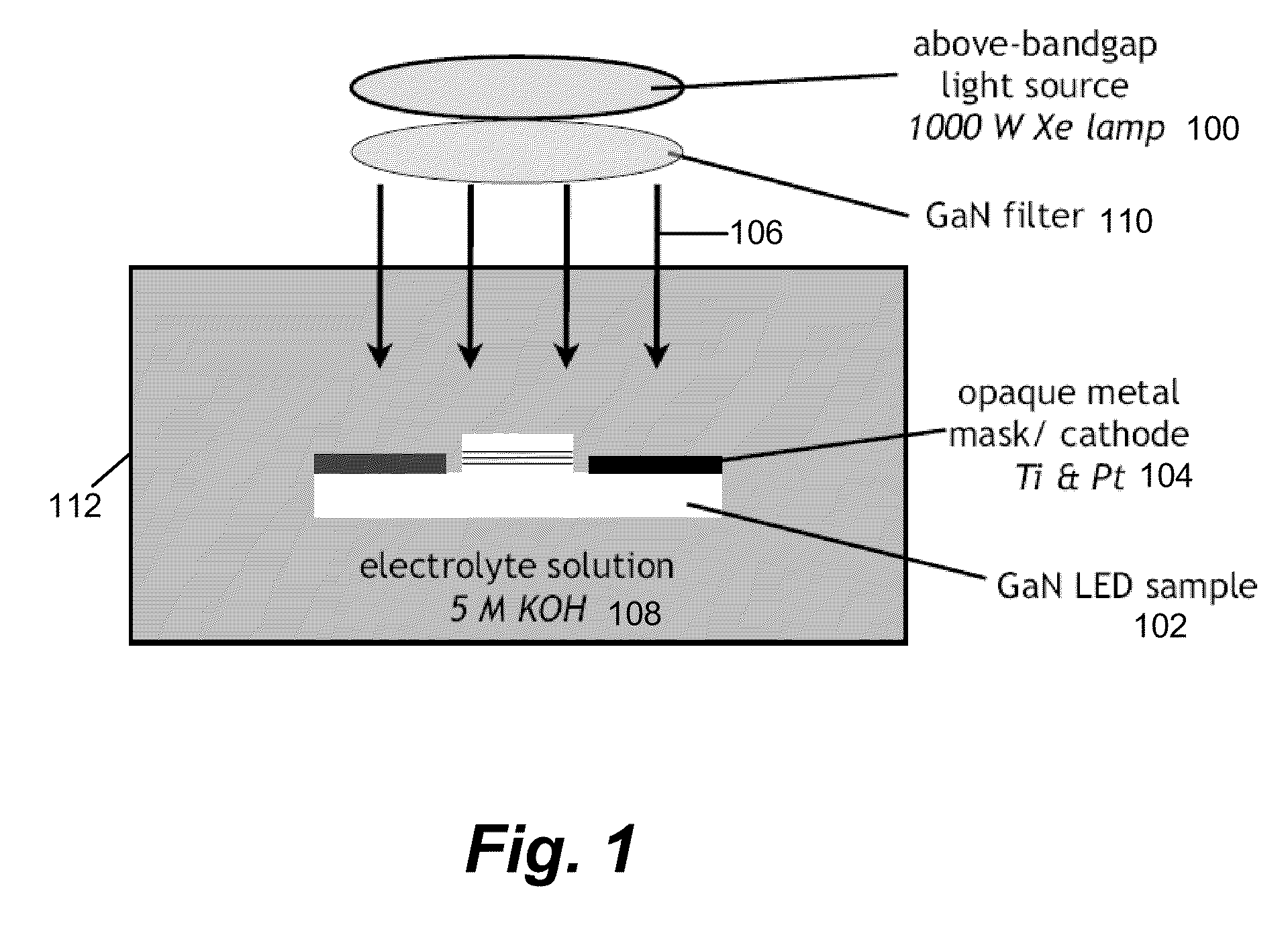
[0040]There have been limited reports of PEC etching of p-type semiconductors in the past, and they have generally required elevated temperatures, a substantial external bias on the system, or a complex experimental apparatus. In addition, etch rates are generally very slow compared to n-type materials.

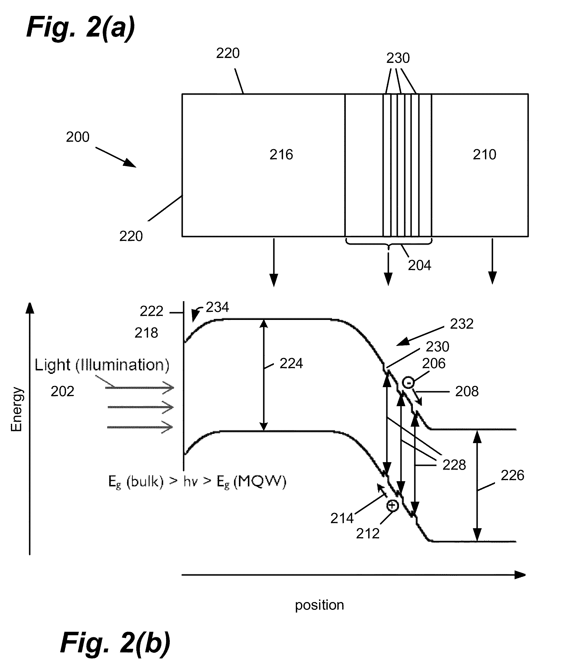
[0041]The key requirements are: (a) there must be a driving force for holes to move towards the surface, rather than the bulk, of the p-type layer, and (b) electron-hole pairs must be generated in a separate area of the structure than the surface to be etched.

[0042]For example, using ...


PUM


Abstract

A method for photoelectrochemical (PEC) etching of a p-type semiconductor layer simply and efficiently, by providing a driving force for holes to move towards a surface of a p-type cap layer to be etched, wherein the p-type cap layer is on a heterostructure and the heterostructure provides the driving force from an internal bias generated internally in the heterostructure; generating electron-hole pairs in a separate area of the heterostructure than the surface to be etched; and using an etchant solution to etch the surface of the p-type layer.

Description

CROSS REFERENCE TO RELATED APPLICATIONS[0001]This application claims the benefit under 35 U.S.C. Section 119(e) of co-pending and commonly-assigned U.S. Provisional Patent Application Ser. No. 61 / 052,421, filed on May 12, 2008, by Adele Tamboli, Evelyn L. Hu, Mathew C. Schmidt, Shuji Nakamura, and Steven P. DenBaars, entitled “PHOTOELECTROCHEMICAL ETCHING OF P-TYPE SEMICONDUCTOR HETEROSTRUCTURES,”;[0002]which application is incorporated by reference herein.[0003]This application is related to the following co-pending and commonly-assigned U.S. patent applications:[0004]U.S. Utility application Ser. No. 10 / 581,940, filed on Jun. 7, 2006, by Tetsuo Fujii, Yan Gao, Evelyn L. Hu, and Shuji Nakamura, entitled “HIGHLY EFFICIENT GALLIUM NITRIDE BASED LIGHT EMITTING DIODES VIA SURFACE ROUGHENING,”, now U.S. Pat. No. 7,704,763, issued Apr. 27, 2010, which application claims the benefit under 35 U.S.C Section 365(c) of PCT Application Serial No. US2003 / 039211, filed on Dec. 9, 2003, by Tetsuo...

Claims


Application Information

Patent Timeline
Patent Type & Authority Patents(United States)
IPC IPC(8): H01L21/3213
CPCH01L21/30617H01L29/2003H01L33/0075
Inventor TAMBOLI, ADELEHU, EVELYN LYNNSCHMIDT, MATHEW C.NAKAMURA, SHUJIDENBAARS, STEVEN P.
Owner RGT UNIV OF CALIFORNIA
Why Eureka
Try Eureka