Apparatus and method for amplifying signal power in a communication system
Inactive Publication Date: 2011-11-08
SAMSUNG ELECTRONICS CO LTD
View PDF4 Cites 1 Cited by
Summary
Abstract
Description
Claims
Application Information
AI Technical Summary
This helps you quickly interpret patents by identifying the three key elements:
Problems solved by technology
Method used
Benefits of technology
Benefits of technology
[0024]Another aspect of the present invention is to provide a signal power amplification apparatus and method in which operating bandwidths of hardware modules in a transmitter are reduced in a communication system.
[0025]Further another aspect of the present invention is to provide a signal power amplification apparatus and method for preventing an increase in non-linearity in a communication system.
Problems solved by technology
In addition, as the operating bandwidth increases, the transmitter using the EER scheme increases in non-linearity caused by the transmission signal's power amplification due to the limitation on implementing a digital-to-analog converter (DAC) and the limitation on implementing the bias modulator because of the limit and loss of switching frequency of the switching elements.
Method used
Image
Click on the blue label to locate the original text in one second.
Reading with bidirectional positioning of images and text.
Examples
first embodiment
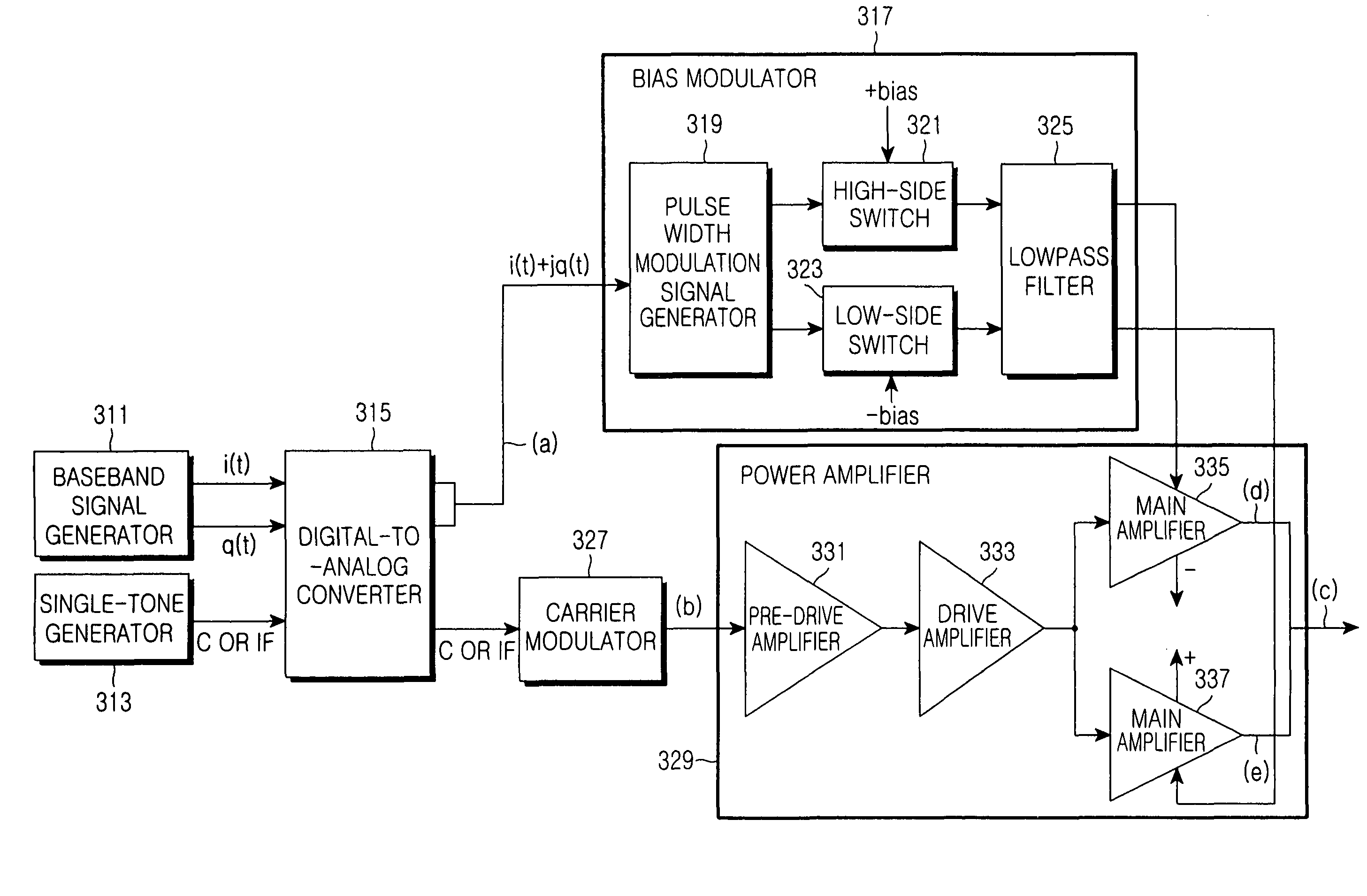
[0039]FIG. 3 is a diagram illustrating a structure of a transmitter using a power amplification scheme based on the present invention.
[0040]Referring to FIG. 3, a transmitter includes a baseband signal generator 311, a single-tone generator 313, a digital-to-analog converter 315, a bias modulator 317, a carrier modulator 327, and a power amplifier 329.
[0041]The baseband signal generator 311 generates a baseband signal including an in-phase (I) component and a quadrature (Q) component having a 90°-phase difference. The baseband signal generated by the baseband signal generator 311 is a digital signal.
[0042]The single-tone generator 313 generates a single-tone signal for carrier modulation (for example, a constant signal having a fixed amplitude or an intermediate frequency (IF) signal). The IF signal generated by the single-tone generator 313 can be, for example, an IF sine wave signal. The single-tone signal generated by the single-tone generator 313 is a digital signal.
[0043]The di...
second embodiment
[0064]FIG. 4 is a diagram illustrating a structure of a transmitter using a power amplification scheme based on the present invention.
[0065]Referring to FIG. 4, the transmitter includes a baseband signal generator 411, a single-tone generator 413, a digital-to-analog converter 415, a bias modulator 417, a carrier modulator 429, and a power amplifier 431.
[0066]The bias modulator 417 includes a pulse width modulation signal generator 419, a serial-to-parallel converter 421, at least two high-side switches 423, at least two low-side switches 425, and a low-pass filter 427.
[0067]The power amplifier 431 includes a pre-drive amplifier 433, a drive amplifier 435, a first main amplifier 437, and a second main amplifier 439.
[0068]This transmitter is different from the transmitter shown in FIG. 3 in terms of the structure of the bias modulator 417.
[0069]For the operations of devices such as the baseband signal generator 411, the single-tone generator 413, the digital-to-analog converter 415, ...
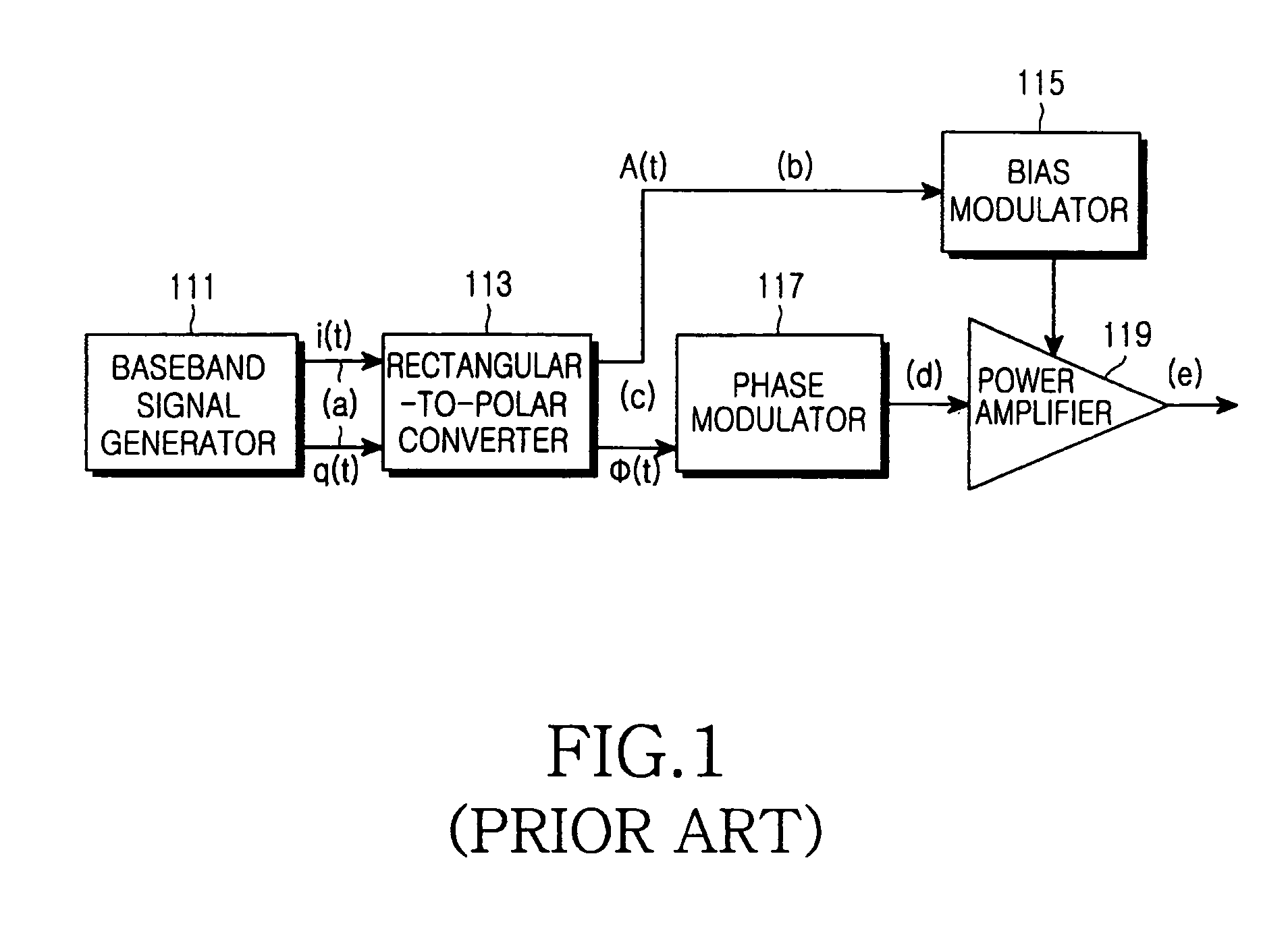
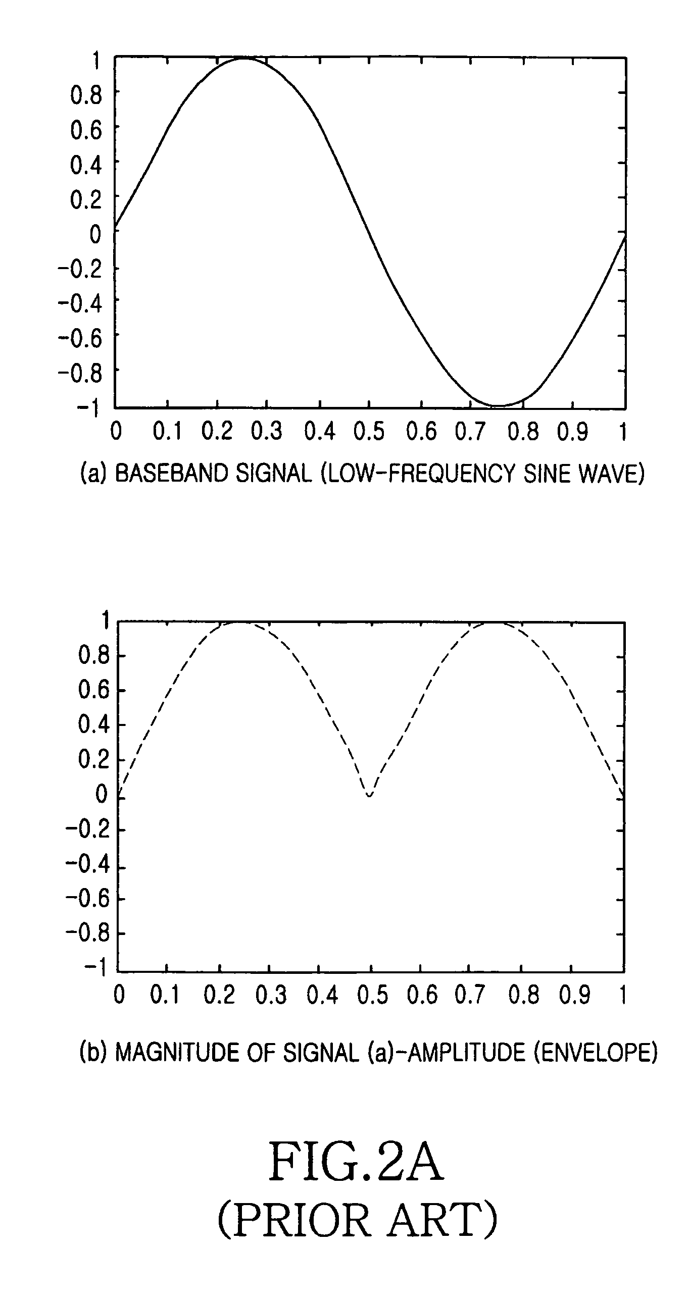
CROSS-REFERENCE TO RELATED APPLICATION(S) AND CLAIM OF PRIORITY[0001]The present application claims the benefit under 35 U.S.C. §119(a) of a Korean patent application filed in the Korean Intellectual Property Office on Jan. 11, 2008 and assigned Serial No. 10-2008-0003672, the entire disclosure of which is hereby incorporated by reference.TECHNICAL FIELD OF THE INVENTION[0002]The present invention relates generally to a communication system and, in particular, to an apparatus and method for amplifying signal power in a communication system.BACKGROUND OF THE INVENTION[0003]A communication system has a power amplifier, included in a transmitter, for amplifying transmission signals during signal transmission, and the transmitter power-amplifies transmission signals by means of the power amplifier and transmits the power-amplified signals.[0004]Currently, communication systems are increasingly evolving, and due to the evolution of communication systems, the transmitter increasingly requ...
Claims
Application Information
Patent Timeline
Application Date:The date an application was filed.
Publication Date:The date a patent or application was officially published.
First Publication Date:The earliest publication date of a patent with the same application number.
Issue Date:Publication date of the patent grant document.
PCT Entry Date:The Entry date of PCT National Phase.
Estimated Expiry Date:The statutory expiry date of a patent right according to the Patent Law, and it is the longest term of protection that the patent right can achieve without the termination of the patent right due to other reasons(Term extension factor has been taken into account ).
Invalid Date:Actual expiry date is based on effective date or publication date of legal transaction data of invalid patent.

