Nanostructure for molecular electronics comprising collinear metal lines defining precise nanoscale gap

a nanoscale gap and collinear metal technology, applied in the direction of nanoinformatics, thermoelectric devices, semiconductor/solid-state device details, etc., can solve the problems of inconvenient use, waste of time, and inability to accurately define the nanoscale gap,

Active Publication Date: 2011-11-15
AVIRAM ARI
View PDF4 Cites 0 Cited by
  • Summary
  • Abstract
  • Description
  • Claims
  • Application Information

AI Technical Summary

Benefits of technology

[0040]What is left on the surface is the pattern shown in FIG. 2e, which contains gaps whose dimensions are of the required thickness, matching the thickness of the sacrificial layer. In this way the sacrificial film controls the distance between the structure pairs.

Problems solved by technology

The problem is particularly acute when the necessary patterns are of nanometer size.
However, according to Kelly; Roberta, in “Electron Beam Lithography” the results can be imprecise because of uneven distribution of the resist on the wafer surface, which results in improper focusing of the electron beam and imprecise deviations of line thickness' from what is desired.
Since current methods for preparing nanometer-size structures are not precise, the structures are created by a hit-or-miss type of technique.
This imprecise technique is wasteful and time-consuming, and it is not suited for manufacturing processes.
While structures containing 4-nm size gaps have been obtained using the above described technique (such as in FIG. 1b herein), the process for fabricating them is complicated.

Method used


Image

  • Nanostructure for molecular electronics comprising collinear metal lines defining precise nanoscale gap
  • Nanostructure for molecular electronics comprising collinear metal lines defining precise nanoscale gap
  • Nanostructure for molecular electronics comprising collinear metal lines defining precise nanoscale gap

Examples


example 1

[0070]The following nonlimiting examples are presented to illustrate the present invention.

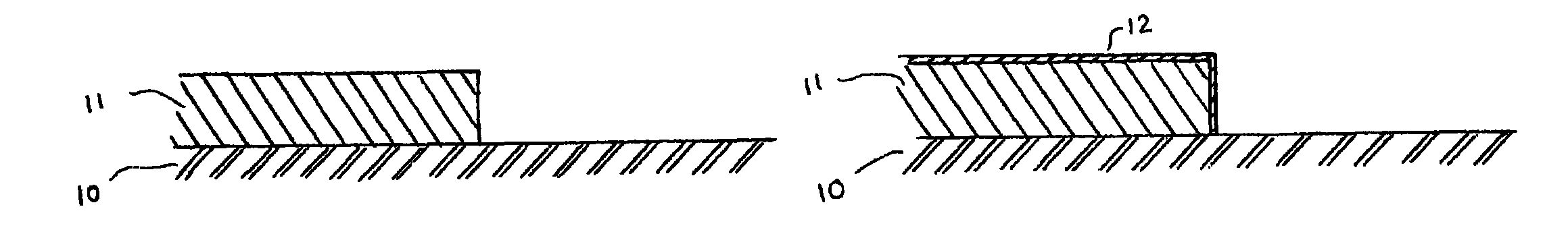
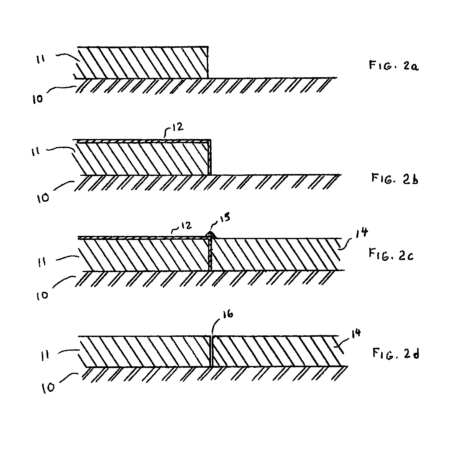
[0071]A silicon wafer is provided and uniformly coated with a silicon dioxide layer, 1000-angstroms thick.

[0072]The wafer is coated with a layer of HMDS.

[0073]The wafer is coated with a layer of e-beam resist composed of PMMA 8.5% MMA copolymer, followed by a layer of PMMA e-beam resist. The bilayer structure permits liftoff metal deposition in a later step. The resist is exposed by e-beam lithography as is known in the art and developed with a methylisobutyl ketone / isopropanol 1:1 mixture. A pattern is produced in the resist film. A short step of reactive ion etching is used to remove any scum left over in the developed areas, and the exposed HMDS film.

[0074]The surface containing the developed film pattern is coated with a film of gold, which is half as thick as the resist film, and the excess metal film is removed by liftoff together with the residual resist. A gold pattern remains on the s...

example 2

[0080]The procedure of Example 1 is used to produce a platinum-gap-platinum pattern.

example 3

[0081]The process of Example 1 is used with a sacrificial layer made of zirconium oxide.


PUM

PropertyMeasurementUnit
gap lengthaaaaaaaaaa
gap widthaaaaaaaaaa
thicknessaaaaaaaaaa

Abstract

A nanostructure pattern which includes pairs of metal lines separated by identical gaps whose dimensions are in the nanometer range, can be prepared by providing a separating sacrificial layer, whose dimensions can be controlled precisely, in the separation gap between the first metal line and the second metal line. The sacrificial layer is removed at the end of the fabrication, leaving a precisely dimensioned gap between the lines.

Description

TECHNICAL FIELD[0001]The present invention is concerned with materials and methods for producing patterns of conductive wires, semiconducting and insulating structures with nanometer-size gaps. The patterns are needed in various areas of technology, but most importantly in the area of nanotechnology for preparing quantum dots and other quantum devices, and for wiring molecular devices for molecular electronics, including carbon nanotubes or other nanotubes. It is very important to be able to prepare such structures efficiently and reliably with consistent results. The present invention makes it possible to fabricate precise nanometer-size structures.BACKGROUND ART[0002]The fabrication of patterned devices often requires high-precision lithography. As the dimensions of the features decrease, so do the number of techniques available for fabricating them. The problem is particularly acute when the necessary patterns are of nanometer size. In this case, the only lithography available is...

Claims


Application Information

Patent Timeline
Patent Type & Authority Patents(United States)
IPC IPC(8): H01L29/41H01L51/10
CPCB82Y10/00B82Y40/00H01L21/76838Y10S977/721Y10S977/932
Inventor AVIRAM, ARI
Owner AVIRAM ARI
Why Eureka
Try Eureka