Circuits and methods allowing for pixel array exposure pattern control

a pixel array and exposure pattern technology, applied in the field of image processing systems, image sensor circuits, pixel circuits, image processing methods, etc., can solve the problems of inability to see objects in the bright areas of images, accumulating too much charge or accumulating too little charge as described above, and unable to see objects in the dark areas. , to achieve the effect of reducing the risk of pixel circuit failure, reducing the risk of pixel failure, and reducing the effect o

Inactive Publication Date: 2011-11-22
INNOVACIONES MICROELECTRONICSAS +1
View PDF26 Cites 11 Cited by
  • Summary
  • Abstract
  • Description
  • Claims
  • Application Information

AI Technical Summary

Benefits of technology

[0034]A method in an image sensor circuit in accordance with an embodiment of the present invention includes (a) starting an integration of charge in each of a plurality of pixel circuits of a pixel array of the image sensor circuit; (b) preventing the integration of charge in at least a particular pixel circuit of the plurality of pixel circuits that is selected based at least partially on one or more signals output from the pixel array; and (c) preventing the integration of charge in at least one pixel circuit of the plurality of pixel circuits that is adjacent to the particular pixel circuit in the pixel array based at least partially on a dilation rule.
[0037]Various embodiments of the present invention allow for controlling a pixel array using feedback, such that the pixel array is controlled based at least partially on signals output from the pixel array that are indicative of charge that has already accumulated in at least a portion of the pixel array during an image capture operation. Also, various embodiments of the present invention allow for controlling a duration of integration time at an individual pixel circuit level, such that pixel circuits in a same row of the pixel array may each integrate charge for different amounts of time during an image capture operation. In various embodiments, a particular shutter operation allows for causing pixel circuits that are integrating charge for a bright area of a physical scene to integrate charge for a shorter integration time than an integration time of pixel circuits that are integrating charge for darker areas of the physical scene. Therefore, various embodiments of the present invention provide for controlling an amount of time that individual pixel circuits are allowed to accumulate charge during an image capture operation based at least partially on charge already accumulated by pixel circuits during the image capture operation.

Problems solved by technology

Related art image sensor circuits that place an emphasis on realistic depictions of scenes for human viewing may create some problems when used for pattern recognition applications.
However, attempting to preserve a relative relationship between points of light intensity in a scene may lead to problems when capturing an image of a high dynamic range scene for pattern recognition purposes, because a variation in light intensity in the physical scene may exceed a dynamic range of the pixel circuits.
Such a saturation of charge may lead to an inability to see objects in the bright areas of the image.
On the other hand, if the integration time for accumulating charge in such a case with a global shutter or rolling shutter operation is set to be a short time so as not to saturate the pixel circuits accumulating charge for the bright areas, then pixel circuits accumulating charge for the dark areas may not accumulate enough charge to allow for seeing objects in the dark areas.
The problem of accumulating too much charge or accumulating too little charge as described above can be very serious in the context of automated pattern recognition, because it is difficult and often impossible to recognize an object that cannot be seen in an image.
For instance, in the example provided above, if captured images were being used to automatically control a car that is driving in the tunnel, then having a saturation of an image at the exit area of the tunnel may prevent the ability to recognize objects at the exit of the tunnel, which would adversely impact an ability to avoid such objects with the car.
Thus, the global shutter and rolling shutter operations may lead to problems in cases of capturing images of high dynamic range scenes that have large differences in light intensity between different areas of the scenes.
Such problems may prevent objects or patterns from being recognized in images captured by the image sensor circuit 100.

Method used


Image

  • Circuits and methods allowing for pixel array exposure pattern control
  • Circuits and methods allowing for pixel array exposure pattern control
  • Circuits and methods allowing for pixel array exposure pattern control

Examples


Embodiment Construction

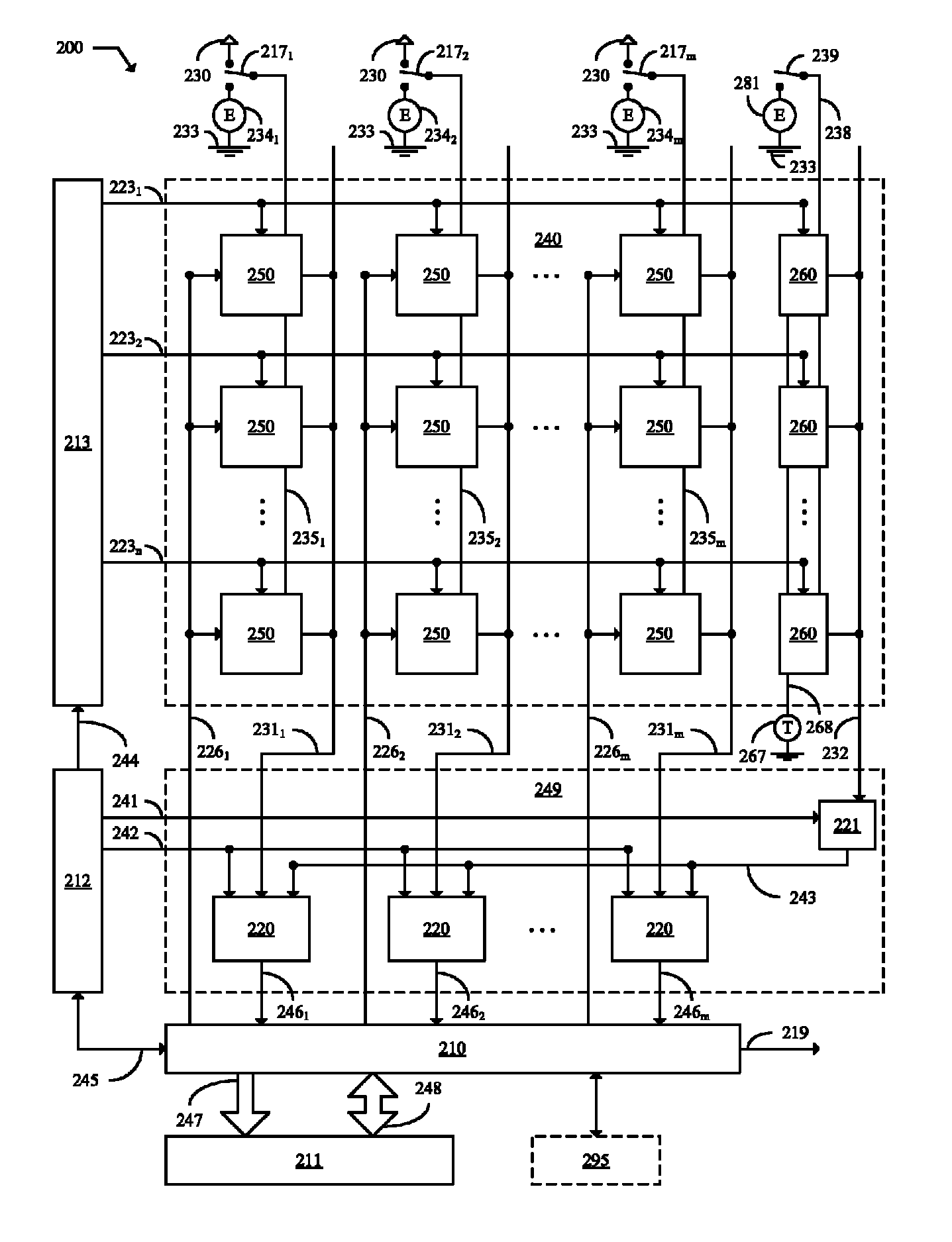
[0073]FIG. 5 illustrates a block diagram of an image processing system 700 in accordance with an embodiment of the present invention. The image processing system 700 includes an image sensor circuit 200 and a processor 800. The image sensor circuit 200 includes a pixel array 240 and one or more circuits 290. In various embodiments, the image sensor circuit 200 and the processor 800 are both located on a single chip. In various embodiments, the image sensor circuit 200 allows for capturing images of physical scenes, and the processor 800 is configured to process the images captured by the image sensor circuit 200. In some embodiments, the processor 800 is configured to receive data for an image from the image sensor circuit 200 and is configured to processes the data to detect one or more objects in the image. In various embodiments, the image processing system 700 may be used for machine vision or other automated pattern recognition applications. In some embodiments, the image proce...


PUM


Abstract

An image processing system includes an image sensor circuit. The image sensor circuit is configured to obtain an image using a type of shutter operation in which an exposure pattern of a pixel array is set according to exposure information that changes over time based at least partially on charge accumulated in at least a portion of the pixel array. An image sensor circuit includes a pixel array and one or more circuits. The one or more circuits are configured to update exposure information based at least partially on one or more signals output from the pixel array, and to control an exposure pattern of the pixel array based on the exposure information. A pixel circuit includes a first transistor connected between a photodiode and a sense node, and a second transistor connected between an exposure control signal line and a gate of the first transistor.

Description

CROSS-REFERENCE TO RELATED PATENT APPLICATIONS[0001]This application claims the benefit of U.S. Provisional App. Ser. No. 60 / 953,905, entitled “CMOS Imager”, filed Aug. 3, 2007, and this application also claims the benefit of U.S. Provisional App. Ser. No. 61 / 020,560, entitled “CMOS Image Sensor for Machine Vision”, filed Jan. 11, 2008, the entire contents of both of which are incorporated by reference herein.BACKGROUND INFORMATION[0002]1. Field of the Invention[0003]Embodiments of the present invention relate generally to image processing systems, image sensor circuits, pixel circuits, image capturing methods, and image processing methods and, in specific embodiments, to an image sensor circuit including a pixel array and one or more circuits for controlling pixel circuits of the pixel array.[0004]2. Related Art[0005]Image sensor circuits are widely used to obtain images of physical scenes and objects. In many instances, image sensor circuits are employed to obtain images that are ...

Claims


Application Information

Patent Timeline
Patent Type & Authority Patents(United States)
IPC IPC(8): H01L27/00H01L31/00H04N3/14H04N5/335
CPCH04N5/2353H04N5/378H04N5/35554H04N5/3535H04N23/73H04N25/533H04N25/583H04N25/75
Inventor MCGARRY, E. JOHNDOMINGUEZ-CASTRO, RAFAELGARCIA, ALBERTO
Owner INNOVACIONES MICROELECTRONICSAS
Why Eureka
Try Eureka