

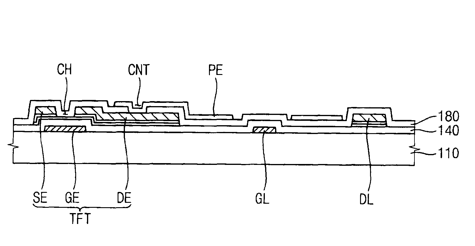
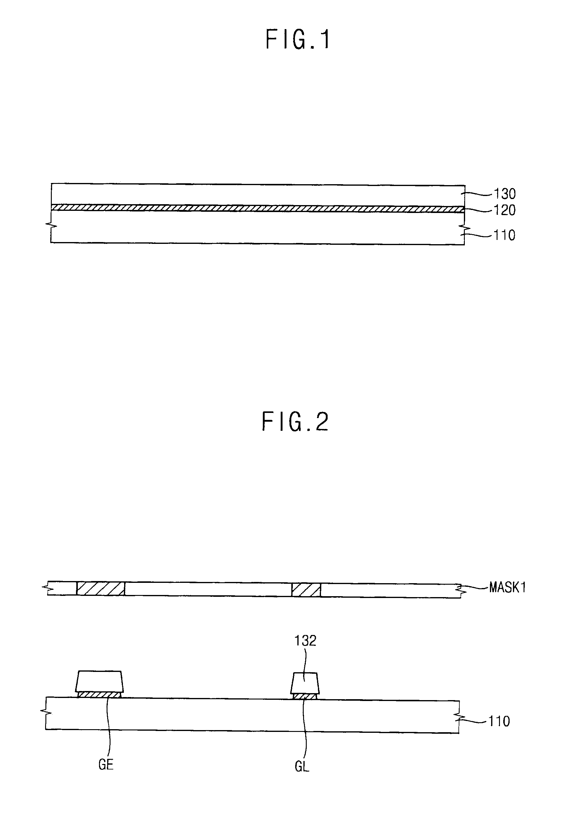
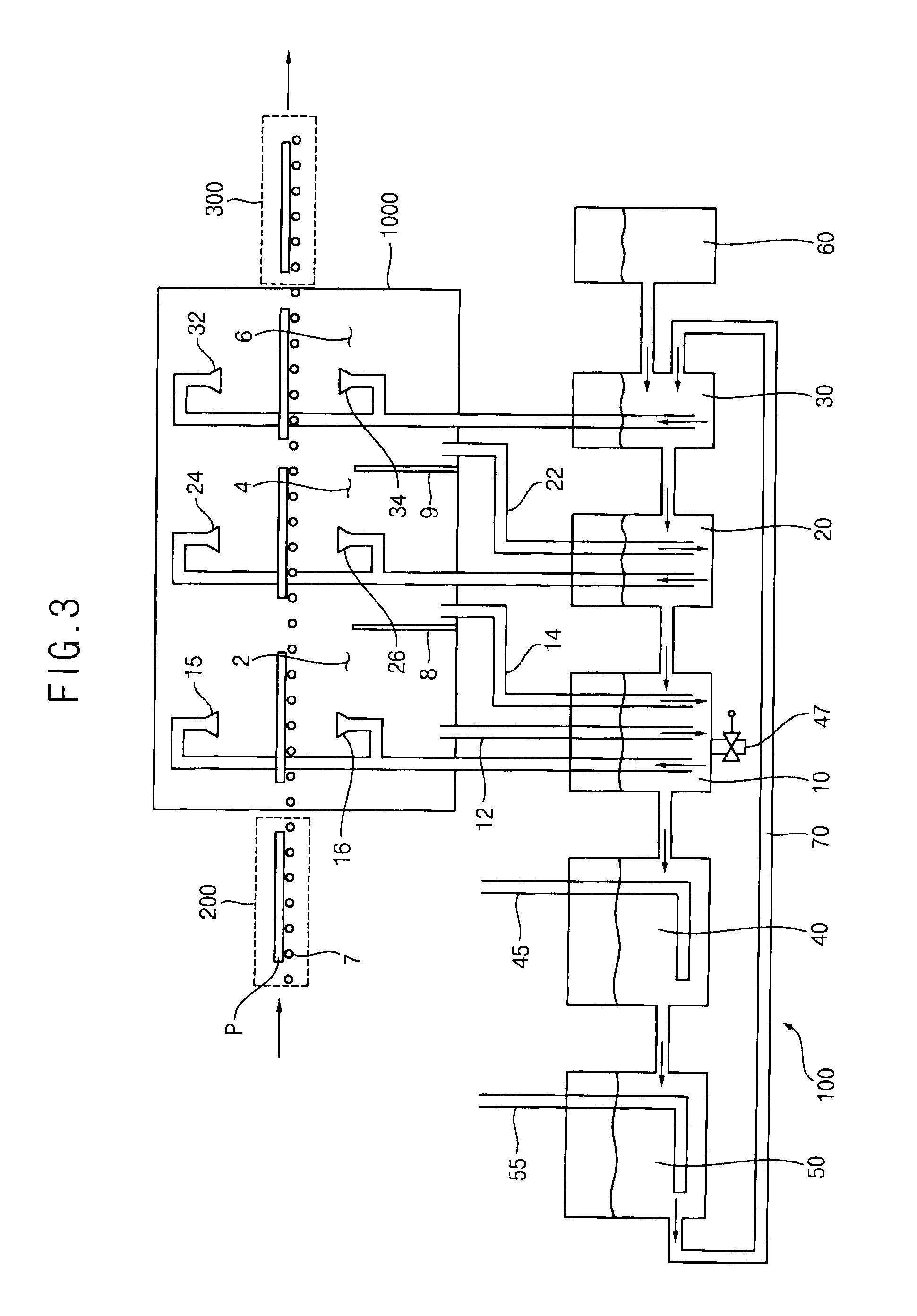
Composition for removing photoresist and method of manufacturing an array substrate using the same
a technology of photoresist and array substrate, which is applied in the direction of photosensitive materials, instruments, photomechanical equipment, etc., can solve the problems of heavy corrosion of metal thin layers, prevent and/or reduce the corrosion of metal layers formed under photoresist, and improve the ability of removing photoresist. , the effect of improving the ability of removing photoresis
- Summary
- Abstract
- Description
- Claims
- Application Information
AI Technical Summary
Benefits of technology
Problems solved by technology
Method used
Image

Examples
experiment 1
[0048]An aluminum layer, a molybdenum layer and a copper layer, which have a thickness of about 2,000 Å, were formed on a glass substrate, and a photoresist composition was coated on the metal layers and developed to prepare a first sample in order to evaluate a corrosion of a metal layer.
[0049]The first sample was dipped into each compound in Table 1, which was held at a temperature of about 70° C., for about 20 minutes. The results are illustrated in Table 1.
experiment 2
n Removing of a Photoresist
[0050]A chromium layer was formed on a glass substrate, and a photoresist composition was coated on the chromium layer and developed to form a photoresist pattern. The chromium layer was wet-etched by using an etching solution, and an etching gas was provided to the glass substrate to prepare a second sample.
[0051]The second sample was dipped into each compound in Table 1, which was held at a temperature of about 70° C., for about 30 seconds. The results are illustrated in Table 1.
experiment 3
n Removing of a Photoresist
[0052]An etching gas was provided to the second sample of Experiment 2 again to prepare a third sample. Deformation of the third sample due to the etching gas was greater than that of the second sample.
[0053]The third sample was dipped into each compound in Table 1, which was held at a temperature of about 70° C., for about 30 seconds. The results are illustrated in Table 1.
[0054]In Table 1, regarding Experiment 1, “⊚” represents that the sample was not corroded, “∘” represents that the sample was slightly corroded, “Δ” represents that the sample was corroded substantially, and “X” represents that the sample was completely corroded. In Table 1, regarding Experiments 2 and 3, “⊚” represents that the photoresist pattern was completely removed, “∘” represents that a portion of photoresist pattern remained, “Δ” represents that a great portion of photoresist pattern remained, and “X” represents that the photoresist pattern was not removed.
[0055]
TABLE 1Experimen...
PUM
| Property | Measurement | Unit |
|---|---|---|
| temperature | aaaaa | aaaaa |
| weight | aaaaa | aaaaa |
| polar | aaaaa | aaaaa |
Abstract
Description
Claims
Application Information