Electron beam apparatus and image display apparatus using the same

a technology of image display and electron beam, which is applied in the manufacture of electrode systems, electric discharge tubes/lamps, and discharge tubes luminescnet screens, etc., to achieve stable electron emission characteristics, inhibit gate deformation, and stable image display

Inactive Publication Date: 2011-12-27
CANON KK
View PDF29 Cites 0 Cited by
  • Summary
  • Abstract
  • Description
  • Claims
  • Application Information

AI Technical Summary

Benefits of technology

[0006]An object of the present invention is to solve the above-described problem and to prevent the gate from being deformed, thereby reducing variation in the electron emission characteristics and preventing the element from being broken in the electron beam apparatus provided with the laminate-type electron-emitting device.
[0043]The present invention inhibits the deformation of the gate by the Coulomb force between the gate and the cathode generated when driving the electron-emitting device and stable electron emission characteristics may be achieved. Therefore, in the image display apparatus using the electron beam apparatus of the present invention, the stable image display may be maintained.

Problems solved by technology

Also, when the gate is deformed, there is a problem that distance between the gate and the cathode varies to further increase the attracting force between the gate and the cathode and the gate is further deformed.

Method used


Image

  • Electron beam apparatus and image display apparatus using the same
  • Electron beam apparatus and image display apparatus using the same
  • Electron beam apparatus and image display apparatus using the same

Examples


example

First Example

[0146]The electron-emitting device having the configuration illustrated in FIG. 1 was manufactured according to the process in FIGS. 12A to 12G. FIG. 13 is a perspective view thereof.

[0147]First, as illustrated in FIG. 12A, PD200 made of low-sodium glass was used as the substrate 1, a 500 nm-thick SiN (SixNy) film was formed by the sputtering as the insulating layer 22, then a 23 nm-thick SiO2 film was formed by the sputtering as the insulating layer 23. Further, a 30 nm-thick TaN film was formed by the sputtering as the conductive layer 24 on the insulting layer 23.

[0148]Next, after forming the resist pattern on the conductive layer 24 by the photolithography technique, the conductive layer 24 and the insulating layers 23 and 22 were sequentially processed by using the dry etching method, and the insulating member 3 composed of the insulating layers 3a and 3b and the gate 5 were formed as illustrated in FIG. 12B. Since the material to form fluoride was selected in the ...

second example

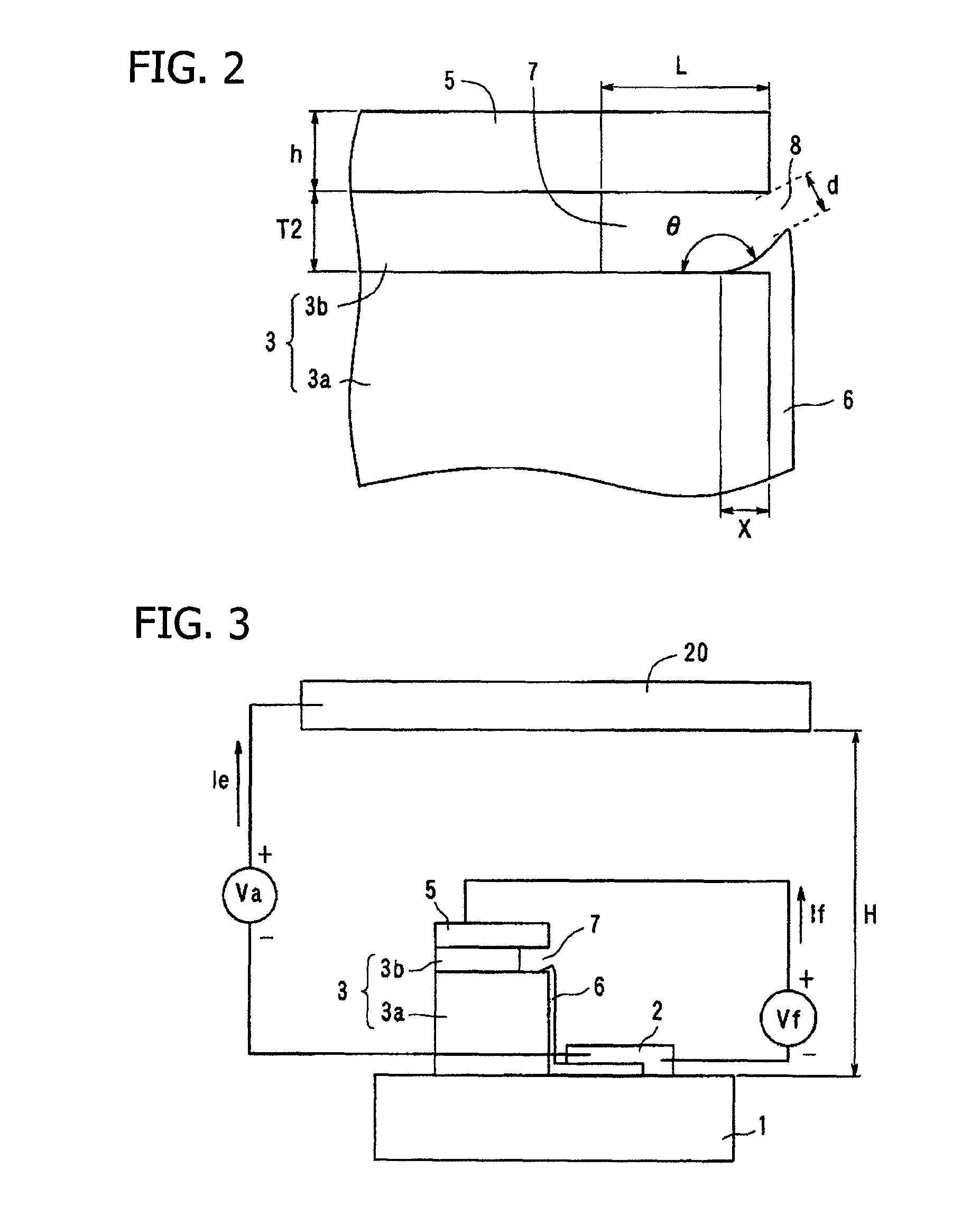
[0157]Next, the electron-emitting device was manufactured in which etching depth of the insulating layer 3b (depth of the concave portion 7) was made shallower than that of the first example, and an effect thereof was studied. Although the made device was similar to that of the first example, the etching depth when forming the concave portion 7 by etching the insulating layer 3b was set to 120 nm. As a result of the analysis by the cross-sectional TEM and the frontal SEM, the distance d of the gap 8 between the protrusion of the cathode 6 being the emitting unit and the gate 5 in FIG. 2 was 3 nm at the minimum and the average value thereof was 14.8 nm. When performing the property evaluation similar to that in the first example using the electron-emitting device thus obtained, as illustrated in FIG. 15, the sudden large current was generated when Vf=30 V.

[0158]In table 1, the configuration of the element, presence or absence of the large current generation, and a value of the upper ...

third example

[0162]The electron-emitting device was manufactured in which the gate 5 was thicker than that in the first example, and the effect thereof was studied. Although the made device was similar to that of the first example, the thickness T2 of the gate 5 was set to 36 nm. As a result of the analysis by the cross-sectional TEM and the frontal SEM, the distance d of the gap 8 between the protrusion of the cathode 6 being the emitting unit and the gate 5 in FIG. 2 was 3 nm at the minimum and the average value thereof was 14.5 nm. When the property evaluation similar to that of the first example was performed by using the electron-emitting device thus obtained, as illustrated in FIG. 16, stable device current was obtained without occurrence of the sudden large current as in the first example in a range in which the voltage up to Vf=26 V was applied.

[0163]In the third example, the upper limit of L / h by the equation (18) when Vf=24 V is represented as

L / h≦4.5  (24-2).

Since L / h=4.29 with L=150 n...


PUM


Abstract

Deformation of a gate by Coulomb force generated when operating an electron-emitting device is inhibited by appropriately maintaining relationship between film thickness h of the gate and distance L from an outer surface of an insulating member to an inner surface of a concave portion. According to this, in an electron beam apparatus provided with a laminate-type electron-emitting device, the deformation of the gate is prevented to reduce variation in electron emission characteristics, thereby preventing the element from being broken.

Description

BACKGROUND OF THE INVENTION[0001]1. Field of the Invention[0002]The present invention relates to an electron beam apparatus provided with an electron-emitting device that emits an electron used in a flat panel display and an image display apparatus using the same.[0003]2. Description of the Related Art[0004]Conventionally, there are electron-emitting devices in which a number of electrons emitted from a cathode collide with an opposed gate and the scattered electrons are taken out. A laminate-type electron-emitting device is one type of such electron-emitting devices, which has a concave portion (recess portion) on an insulating layer in the vicinity of an electron emitting unit and is disclosed in the Japanese Patent Application Laid-Open Publication No. 2001-167693.SUMMARY OF THE INVENTION[0005]In the laminate-type electron-emitting device provided with the concave portion on the insulating layer, attracting force is generated between the gate and the cathode by Coulomb force and ...

Claims


Application Information

Patent Timeline
Patent Type & Authority Patents(United States)
IPC IPC(8): H01J1/62
CPCH01J1/3046H01J3/022H01J9/025H01J31/127H01J2329/0423H01J2329/4613H01J2329/4634
Inventor SUWA, TAKANORIAZUMA, HISANOBUSUMIYA, TOSHIHARU
Owner CANON KK
Why Eureka
Try Eureka