
Semiconductor storage device, method of controlling the same, and error correction system

a technology of semiconductor storage devices and error correction systems, applied in error detection/correction, instruments, coding, etc., can solve problems such as large circuit scale, large probability of occurrence of errors, and mechanism having high error correction capability

Inactive Publication Date: 2011-12-27
KK TOSHIBA
View PDF12 Cites 19 Cited by
  • Summary
  • Abstract
  • Description
  • Claims
  • Application Information

AI Technical Summary

Benefits of technology

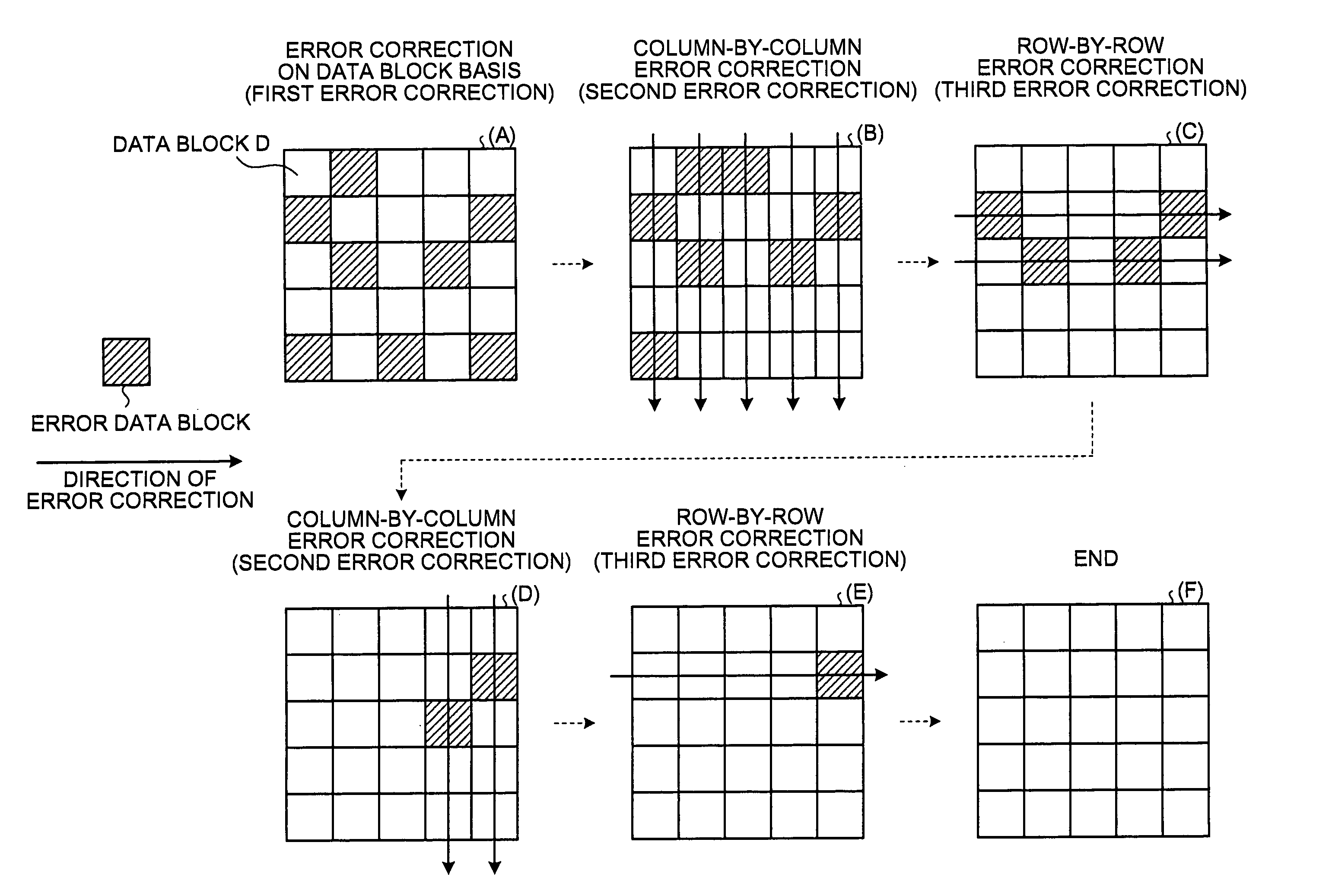
[0010]A method of controlling semiconductor storage device according to another aspect of the present invention includes a host device; and a semiconductor storage device that perform read / write data from / to a nonvolatile memory according to an instruction of the host device, wherein the semiconductor storage device includes a temporary storage unit that divides data transferred from the host device into a plurality of data blocks each formed of a plurality of data, and stores therein the data blocks in a matrix; an error-detection-code generating unit that generates an error detection code to detect an error for each data block; a first error-correction-code generating unit that generates a first error correction code to correct an error for each first unit data formed of the data block; a second error-correction-code generating unit that generates a second error correction code to correct an error for each second unit data formed of the data blocks arranged in a column direction; a third error-correction-code generating unit that generates a third error correction code to correct an error for each third unit data formed of the data blocks arranged in a row direction; a nonvolatile semiconductor memory that can store therein the data blocks, generated error detection code, and generated first to third error correction codes; a first error correcting unit that performs first error correction on each of the data blocks using the first error correction code corresponding thereto; a first error detecting unit that detects an error in first error-corrected block using the error detection code corresponding thereto; a second error correcting unit that performs second error correction on an error in the first error-corrected block detected by the first error detecting unit, using the second error correction code corresponding thereto; and a second error detecting unit that detects an error in second error-corrected block using the error detection code corresponding thereto; and a transmitting unit that transmits the second error-corrected data and a result of detection by the second error detecting unit to the host device, and the host device includes a third error correcting unit that performs third error correction on an error in the second error-corrected block, received from the semiconductor storage device, detected by the second error detecting unit, using the third error correction code corresponding thereto.

Problems solved by technology

In the semiconductor memory devices, electric charge is discharged with passage of time, and thus, if the charge is discharged more than the threshold, an error may occur when information is read.
Particularly, a multi-value type of memory device has generally narrow intervals between thresholds, and this causes the probability of occurrence of an error to increase.
The correction mechanism having the high error correction capability requires a large circuit scale, a large power consumption, and a long time for processing.
Therefore, the high-performance error correction mechanism is wastefully used even if the information to be read contains not so many errors.
This leads to wasteful consumption of power for the storage device.
This also forces the storage device to wastefully consume electric power.

Method used


Image

  • Semiconductor storage device, method of controlling the same, and error correction system
  • Semiconductor storage device, method of controlling the same, and error correction system
  • Semiconductor storage device, method of controlling the same, and error correction system

Examples


first embodiment

[0034]the present invention allows reduction of a power consumption and a circuit scale by performing three types of correction coding with different error correction capabilities when error correction coding / decoding is applied to a memory such as a flash memory having a defective bit.

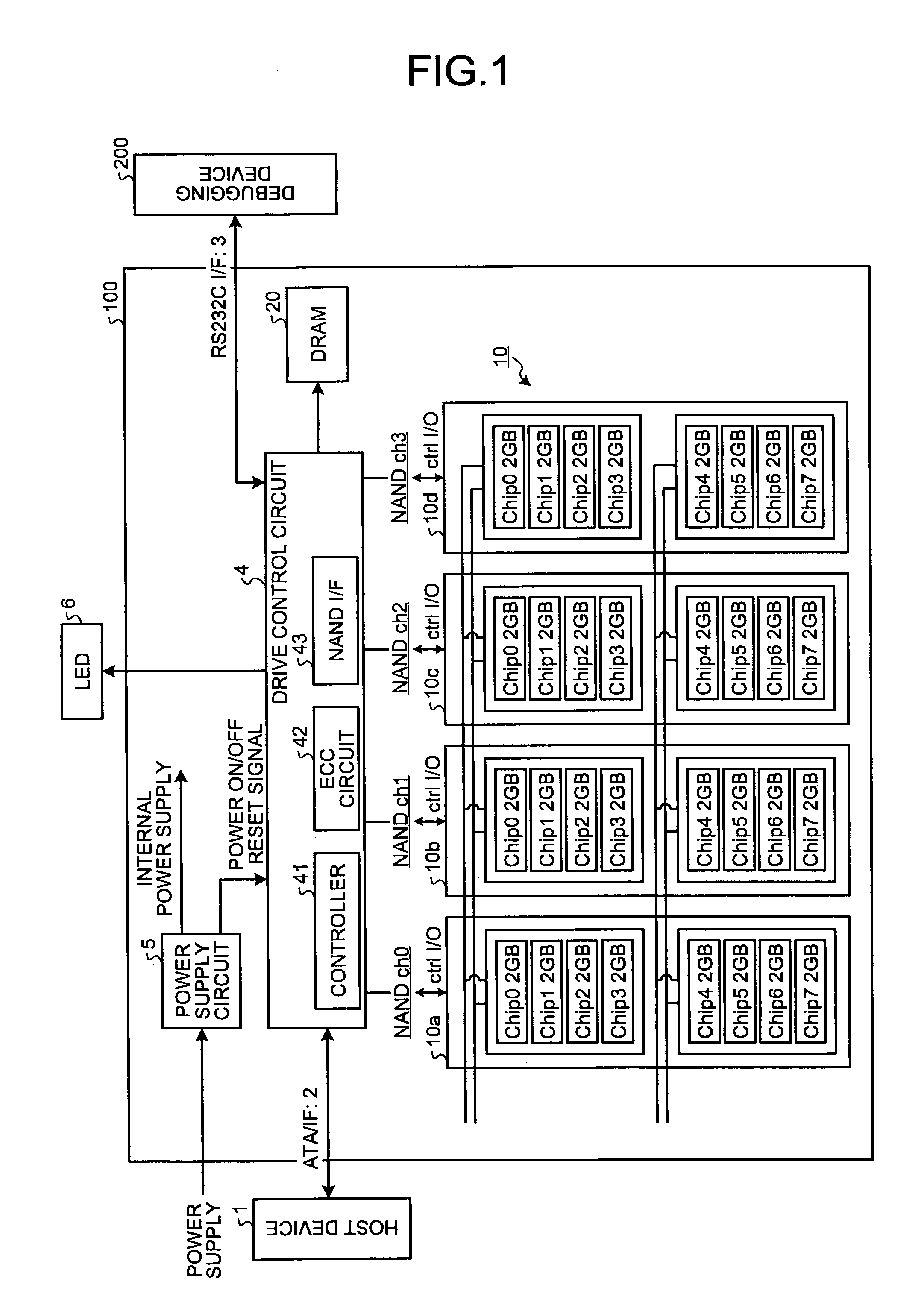
[0035]FIG. 1 is a block diagram of a configuration example of a solid state drive (SSD) 100. The SSD 100 is connected to a host device (host) 1 such as a personal computer or a central processing unit (CPU) core via a memory-connection interface such as an advanced technology attachment (ATA) interface (I / F) (ATA / IF) 2, so that the SSD 100 functions as an external memory of the host device 1. The SSD 100 can perform data transmission / reception with a debugging device 200 via a communication interface 3 such as an RS232C interface (RS232C I / F). The SSD 100 includes a NAND flash memory (hereinafter, “NAND memory”) 10 being a nonvolatile memory, a drive control circuit 4 being a controller, a dynamic ran...

second embodiment

[0129]FIG. 22 is a block diagram of a main portion of a decoding system in an ECC circuit 242 according to the The decoding system of the ECC circuit 242 does not need to incorporate the third ECC correcting unit, and thus, the circuit scale can be reduced.

[0130]According to the second embodiment, because the third error correction is performed by the host device 201, there is no need to perform the third error correction by the SSD 100, which allows reduction in the load on the SSD 100 and in the circuit scale.

[0131]In the second embodiment, the present invention is applied to the SSD having the NAND memory, however, the present invention may be applied to any SSD having other flash electrically erasable programmable read-only memory (EEPROM) such as an NOR type memory.


PUM


Abstract

A semiconductor storage device, a method of controlling the same, and an error correction system allow reduction in power consumption and circuit scale without detriment to error correction capability. An error correction code (ECC) circuit of a solid state drive (SSD) performs first error correction on read data using a first error correction code (Hamming code), and further performs second error correction on the result of the first error correction using a second error correction code (BHC code). Furthermore, the ECC circuit performs third error correction on the result of the second error correction using a third error correction code (RS code).

Description

TECHNICAL FIELD[0001]The present invention relates to a semiconductor storage device, a method of controlling the same, and an error correction system, and more particularly, to a semiconductor storage device including an error correction circuit that corrects an error of a semiconductor memory storing information in a nonvolatile manner, a method of controlling the same, and an error correction system.BACKGROUND ART[0002]Recently, there are widely known semiconductor memory devices such as flash memory that stores information depending on a held charge amount. A multi-value memory technology for storing two bits or more of information by setting a plurality of thresholds of the charge amount is also developed.[0003]In the semiconductor memory devices, electric charge is discharged with passage of time, and thus, if the charge is discharged more than the threshold, an error may occur when information is read. Particularly, a multi-value type of memory device has generally narrow int...

Claims


Application Information

Patent Timeline
Patent Type & Authority Patents(United States)
IPC IPC(8): H03M13/00
CPCG06F11/1012G06F11/1072H03M13/29H03M13/2906G11C16/0483G11C2029/0411G06F11/1044
Inventor YAMAGA, AKIRA
Owner KK TOSHIBA
Learn More