Thyristor semiconductor memory and method of manufacture

Inactive Publication Date: 2012-01-10
T RAM ASSIGNMENT FOR THE BENEFIT OF CREDITORS LLC +1
View PDF34 Cites 44 Cited by
  • Summary
  • Abstract
  • Description
  • Claims
  • Application Information

AI Technical Summary

Benefits of technology

[0008]In yet a further embodiment, the method of fabrication further includes implanting supplemental dopant into a portion of a base region that has been thinned and defined between the cathode region for the thyristor and the underlying buried well. For a device structure of this embodiment, the supplemental dopant provides a concentration of dopant sufficient to avoid depletion width exhaustion of carriers between the cathode region and the underlying buried well.

Problems solved by technology

Memory has become the critical bottleneck in most systems ranging from servers to routers to communications equipments.
For example, the Internet revolution dramatically accelerated network performance requirements, but the technological limits of dynamic random access memory (DRAM) and static random access memory (SRAM) have created a bottleneck defined by the slow speed of DRAMs and the low density of SRAMs.
System designers have struggled for years to find a solution that successfully matches the density of DRAM with the high speed of SRAM.

Method used


Image

  • Thyristor semiconductor memory and method of manufacture
  • Thyristor semiconductor memory and method of manufacture
  • Thyristor semiconductor memory and method of manufacture

Examples


Embodiment Construction

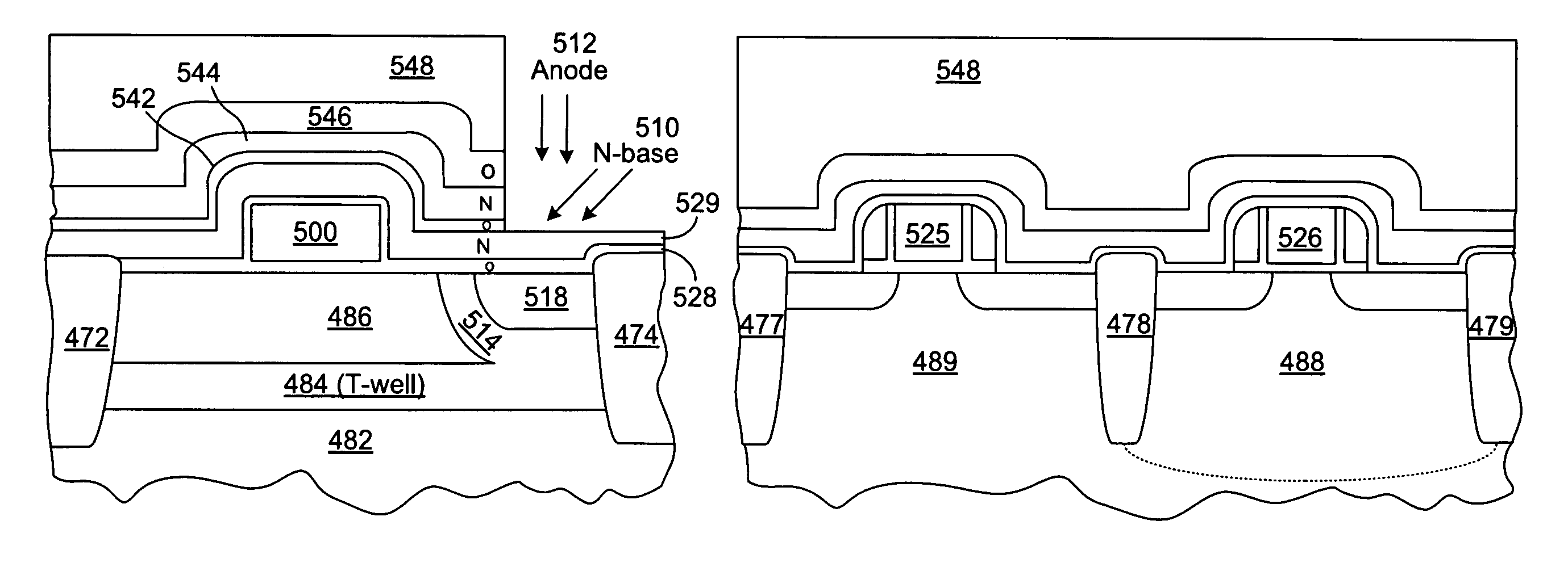
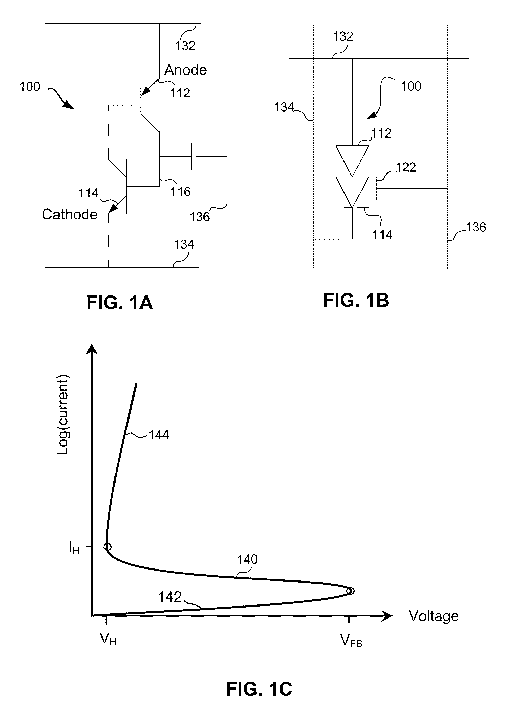
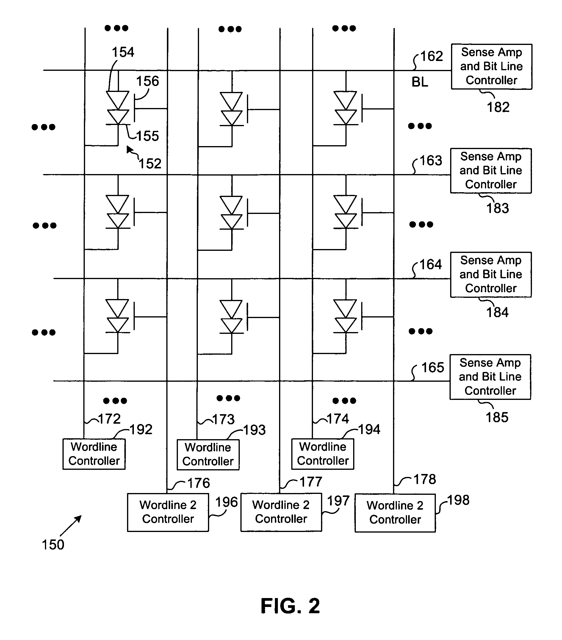
[0033]In the following description, numerous specific details are set forth to provide an understanding of exemplary embodiments of the present invention, wherein similar elements between the various embodiments may be annotated similarly. Additionally, readily established circuits or elements of the exemplary embodiments may be disclosed in simplified form (e.g., simplified block diagrams and / or simplified description) to avoid obscuring an understanding the embodiments with excess detail Likewise, to aid a clear and precise disclosure, description of known structures—e.g., sidewall spacers, gate oxides, conductive lines, voltage sources, contacts, vias, etc.—may similarly be simplified where persons of ordinary skill in this art can readily understand such structures and provisions by way of the drawings and present disclosure.

[0034]Further, it may be understood that the polarity of P and N-type materials for particular examples could be reversed in some embodiments; wherein one e...


PUM


Abstract

A thyristor based semiconductor device includes a thyristor having cathode, P-base, N-base and anode regions disposed in electrical series relationship. The N-base region for the thyristor has a cross-section that defines an inverted “T” shape, wherein a buried well in semiconductor material forms is operable as a part of the N-base. The stem to the inverted “T” shape extends from the upper surface of the semiconductor material to the buried well. The P-base region for the thyristor extends laterally outward from a side of the stem that is opposite the anode region of the thyristor, and is further bounded between the buried well and a surface of the semiconductor material. A thinned portion for the N-base is defined between the cathode region of the thyristor and the buried well, and may include supplemental dopant of concentration greater than that for some other portion of the N-base.

Description

RELATED PATENT DOCUMENTS[0001]This application is a continuation-in-part of U.S. application Ser. No. 11 / 881,159, filed Jun. 25, 2007, which is a continuation-in-part of application Ser. No. 11 / 159,447 filed Jun. 22, 2005. This application also claims benefit of U.S. provisional patent application Ser. No. 60 / 988,607 filed Nov. 16, 2007. All these patent applications are incorporated herein by reference.BACKGROUND[0002]The performance of logic has increased by two orders of magnitude over the past decade while the performance of memory has increased by less than a factor of two. Memory has become the critical bottleneck in most systems ranging from servers to routers to communications equipments. For example, the Internet revolution dramatically accelerated network performance requirements, but the technological limits of dynamic random access memory (DRAM) and static random access memory (SRAM) have created a bottleneck defined by the slow speed of DRAMs and the low density of SRAM...

Claims


Application Information

Patent Timeline
IPC IPC(8): H01L21/332H01L21/337H01L21/8238
CPCG11C11/39H01L27/1027H01L29/66393H01L29/7436
Inventor NEMATI, FARIDROBINS, SCOTTYANG, KEVIN J.
Owner T RAM ASSIGNMENT FOR THE BENEFIT OF CREDITORS LLC
Why Eureka
Try Eureka