Edge removal of films using externally generated plasma species

a plasma species and film technology, applied in the direction of chemical vapor deposition coating, coating, electric discharge tube, etc., can solve the problems of deposition uniformity, process integration difficulties, and wet etching may not be desirable in certain applications

Active Publication Date: 2012-01-24
NOVELLUS SYSTEMS
View PDF42 Cites 48 Cited by
  • Summary
  • Abstract
  • Description
  • Claims
  • Application Information

AI Technical Summary

Benefits of technology

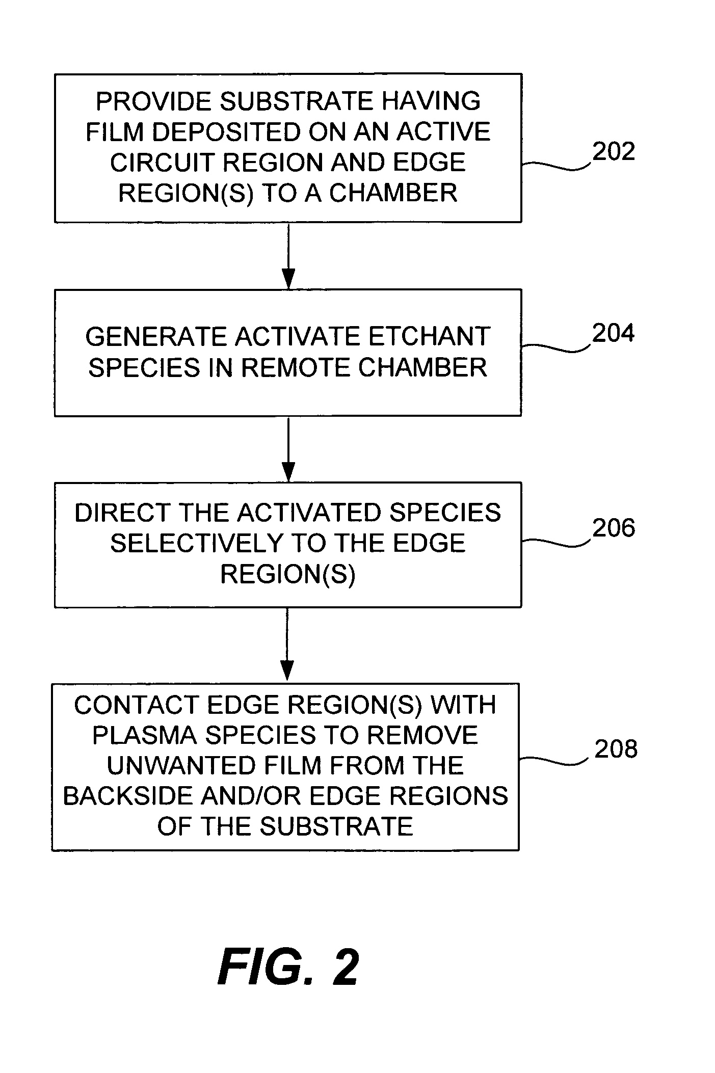
[0006]The present invention meets these needs by providing methods and apparatuses for removing unwanted film from the edge area of substrate using plasmas. In certain embodiments, the plasma is remotely generated. Activated plasma species are directed to the edge of the substrate to contact and remove the unwanted film, while intrusion of the activated

Problems solved by technology

During integrated circuit fabrication, various films are needed on the active circuit region of the wafer, i.e., the main interior region on the front side, but are undesirable elsewhere.
In many cases, deposition of the films beyond the active circuit region creates difficulties in process integration.
However, edge exclusion hardware may not be compatible wi

Method used


Image

  • Edge removal of films using externally generated plasma species
  • Edge removal of films using externally generated plasma species
  • Edge removal of films using externally generated plasma species

Examples


examples

[0064]The following examples are provided to further illustrate aspects and advantages of the present invention. These examples are provided to exemplify and more clearly illustrate aspects of the present invention and are in no way intended to be limiting.

[0065]AHMs of 3500 Angstroms were deposited on substrates by PECVD using a Novellus Vector™ tool on 300 mm wafers.

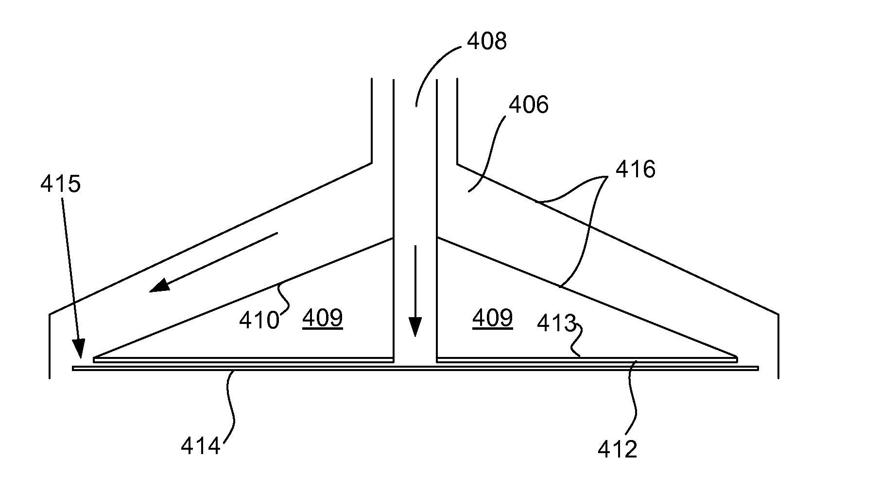
[0066]Edge removal of the unwanted film was then performed using a chamber similar to that depicted in FIG. 3a located in the load lock of the Vector tool. Process conditions and apparatus parameters were as follows:

[0067]Purge Gas: Argon, 750 sccm

[0068]Deflector gap: 0.012 inch

[0069]Etchant Gas Flow: 3.5 L O2+10% N2

[0070]Pressure: 1.5 Torr

[0071]Process time: 2 seconds

[0072]Film was completely removed from the side edge, underside, and front edge of the wafer. FIG. 8 shows a graph comparing AHM thickness profiles of AHMs before and after edge bead removal. As can be seen from the Figure, the edge is completely cleared...


PUM

PropertyMeasurementUnit
Lengthaaaaaaaaaa
Lengthaaaaaaaaaa
Lengthaaaaaaaaaa

Abstract

The present invention provides methods and apparatuses for removing unwanted film from the edge area of substrate using remotely-generated plasmas. Activated plasma species are directed to the edge of the substrate to contact and remove the unwanted film, while intrusion of the activated species to areas above the active circuit region (where the film is desired) is suppressed. In certain embodiments, intrusion of the activated species is suppressed by the use of a purge gas and/or the use of materials that promote recombination of plasma species. In particular embodiments, atomic oxygen is used to remove ashable films from the edge of semiconductor wafers.

Description

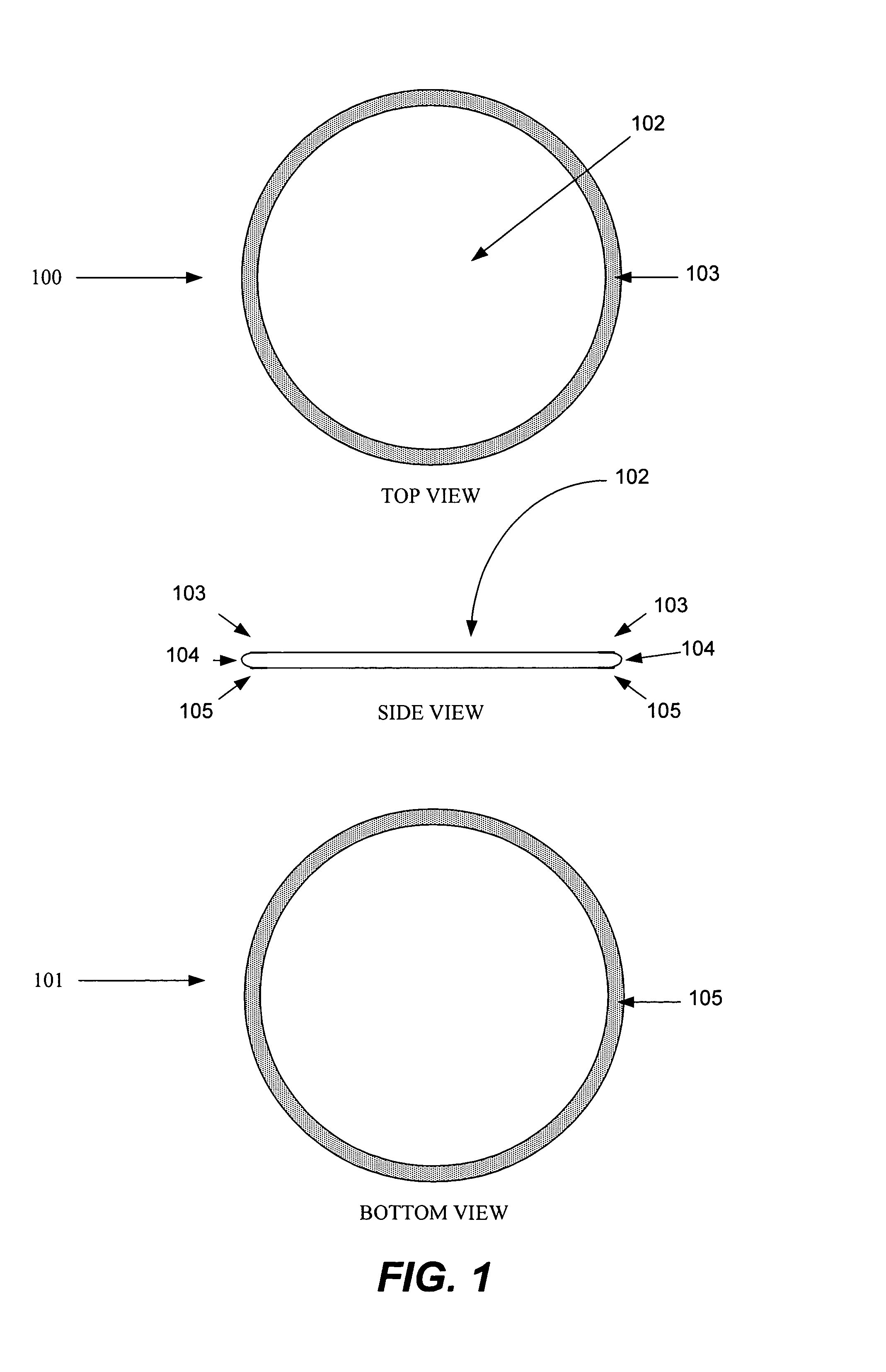
CROSS-REFERENCE TO RELATED APPLICATION[0001]This application is a continuation-in-part of and claims priority to U.S. patent application Ser. No. 11 / 479,353, titled “METHODS FOR REMOVING DEPOSITS FROM THE EDGE OF A SILICON SUBSTRATE USING A PLASMA DISCHARGE,” filed Jun. 30, 2006 now abandoned, which hereby incorporated by reference.FIELD OF THE INVENTION[0002]This invention relates to technology for removing unwanted film from semiconductor wafers. More particularly, it pertains to methods for removing unwanted film, particularly film in the edge regions, using a plasma discharge.BACKGROUND OF THE INVENTION[0003]During integrated circuit fabrication, various films are needed on the active circuit region of the wafer, i.e., the main interior region on the front side, but are undesirable elsewhere. Deposition processes, including chemical vapor deposition (CVD) and physical vapor deposition (PVD) processes, often deposit films out to the edge of the front side of the silicon substrate...

Claims


Application Information

Patent Timeline
IPC IPC(8): C23C16/452C23F1/00C23C16/455H01L21/306C23C16/22C23C16/06
CPCC23F4/00H01J37/32385H01J37/32449H01L21/02087H01L21/31138H01L21/6708
Inventor HENRI, JONMEINHOLD, HENNERGAGE, CHRISTOPHERDOBLE, DAN
Owner NOVELLUS SYSTEMS
Why Eureka
Try Eureka