Semiconductor device

a technology of resistance change and semiconductors, applied in information storage, static storage, digital storage, etc., can solve the problem of difficult manufacture of capacitors for providing sufficient signals, and achieve the effect of increasing the current of rewriting

Inactive Publication Date: 2012-01-24
HITACHI LTD
View PDF4 Cites 15 Cited by
  • Summary
  • Abstract
  • Description
  • Claims
  • Application Information

AI Technical Summary

Benefits of technology

[0011]FIG. 6 shows a first problem to be solved by the present invention. FIG. 6A shows a circuit and a current direction in the case of rewriting a resistance change memory cell MC. A driver V1, a parasitic load RS1, a MC, a parasitic load RS2 and a driver V2 are connected in series, and the rewriting is performed by causing the current I to flow from the V1 to the V2. A parasitic load RP between the driver V1 and the driver V2 is RS1+RS2. FIG. 6B shows a rewriting current I (vertical axis) with respect to RP (horizontal axis). An IC is the lowest current required for operating the MC. In order to operate the MC, the current I equal to or higher than the IC is required. For that purpose, however, the PR has to be reduced to the value within the area shown as target in FIG. 6B. For the reduction of the RP, the RS1 and the RS2 have to be reduced. Particularly, when the MC is in an ON state, since a resistance RM of the memory cell is low, a ratio of RS1+RS2 in the whole resistance components in the current path from the V1 to the V2 increases. Hence, particularly in the rewriting from the ON state to the OFF state, it is important to reduce RS1+RS2. In a large-scale memory array, a long distance wiring is required for the current path from the driver to the memory cell. However, the width of the wiring is reduced with the increase of the integration, and the wiring resistance is increased. Although it is possible to increase the operation voltage to obtain the current necessary for writing, the power consumption increases, so that the reliability of the memory chip is likely to decrease due to heat generation. It is important to reduce the parasitic load in the current path not only by the material, but also by an array configuration and a circuit configuration.
[0015]Therefore, a representative object of the present invention is to provide a technique capable of increasing the rewriting current without increasing the power supply voltage, and at the same time, reducing the location dependency inside the memory array of a resistive state after the rewriting, in the resistance change memory in which the resistance value of the memory cell changes between the logical values “1” and “0”.
[0020]More specifically, as the advantages obtained by the representative embodiment, the rewriting current can be increased without increasing the power supply voltage, and at the same time, the location dependency inside the memory array of a resistive state after the writing can be reduced in the resistance change memory in which the resistance value of the memory cell changes between the logical values “1” and “0”.

Problems solved by technology

The scaling down of the manufacturing rule has been advanced in order to achieve higher integration in a dynamic random access memory (DRAM), but it has become difficult to manufacture a capacitor for providing sufficient signals.

Method used


Image

  • Semiconductor device
  • Semiconductor device
  • Semiconductor device

Examples


first embodiment

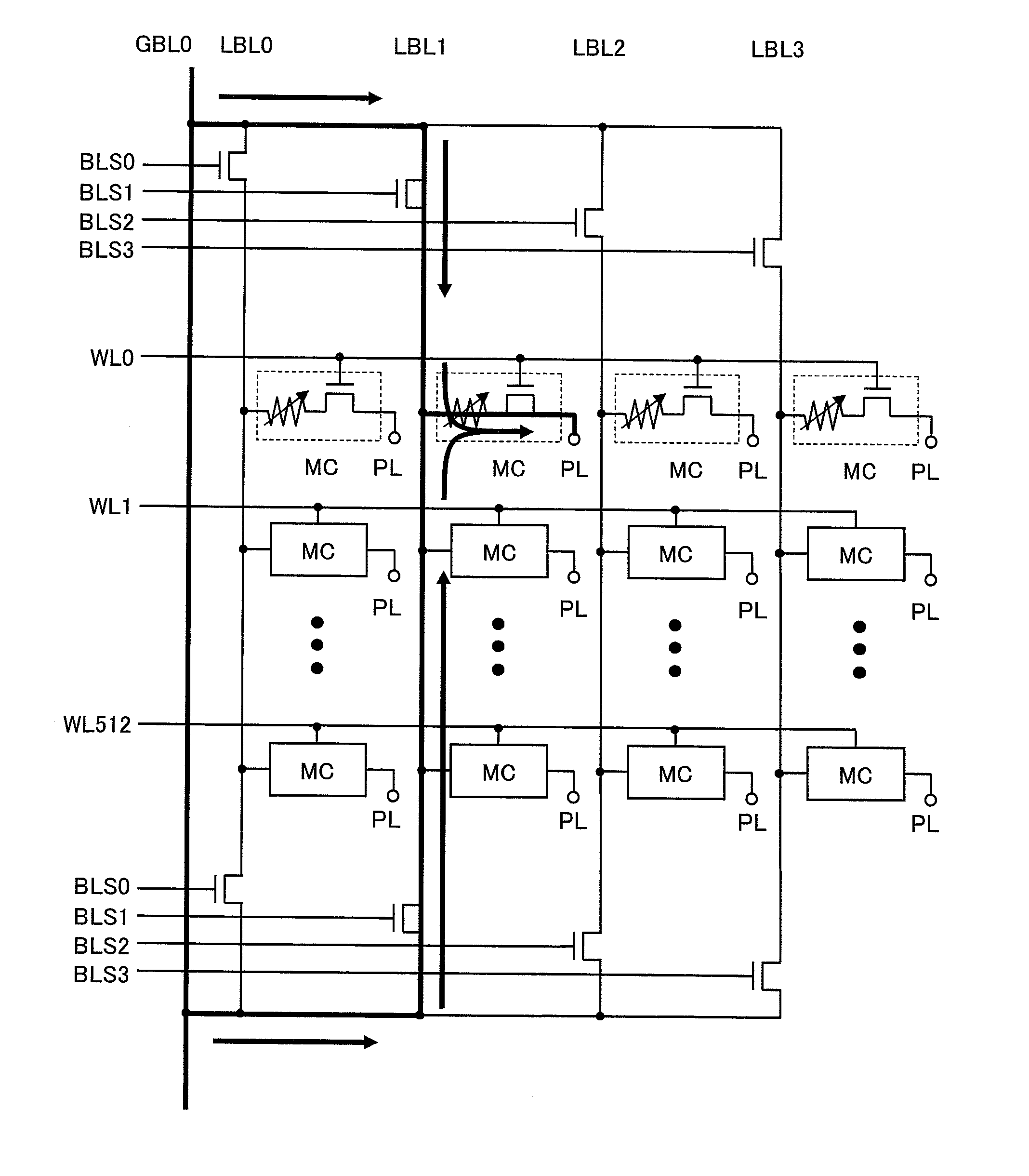
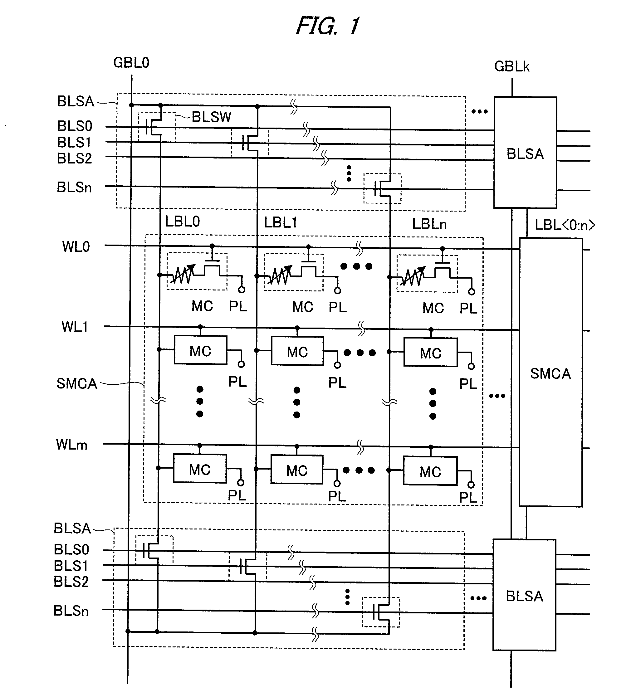
[0070]A semiconductor device according to a first embodiment of the present invention will be described with reference to FIG. 1 and FIG. 8 to FIG. 22.

[0071]FIG. 1 shows one example of the configuration of a memory cell array in the semiconductor device according to the first embodiment.

[0072]The memory cell array is constituted by disposing sub-memory blocks in an array, and the sub-memory block includes upside and downside bit line select switch arrays BLSA having a plurality of bit line select switches BLSW and a sub-memory cell array SMCA adjacently disposed between the upside and downside bit line select switch arrays BLSA and having a plurality of local bit lines LBL (0 to n), a plurality of word lines WL (0 to m) and a plurality of memory cells MC disposed at intersections of the plurality of word lines WL and the plurality of local bit lines LBL.

[0073]The local bit lines LBL are connected to global bit lines GBL (0 to k) in the upside and downside bit line select switch arra...

second embodiment

[0116]A semiconductor device according to a second embodiment of the present invention will be described with reference to FIG. 23 to FIG. 29.

[0117]FIG. 23 shows one example of the operation of a memory cell array in the semiconductor device according to the second embodiment.

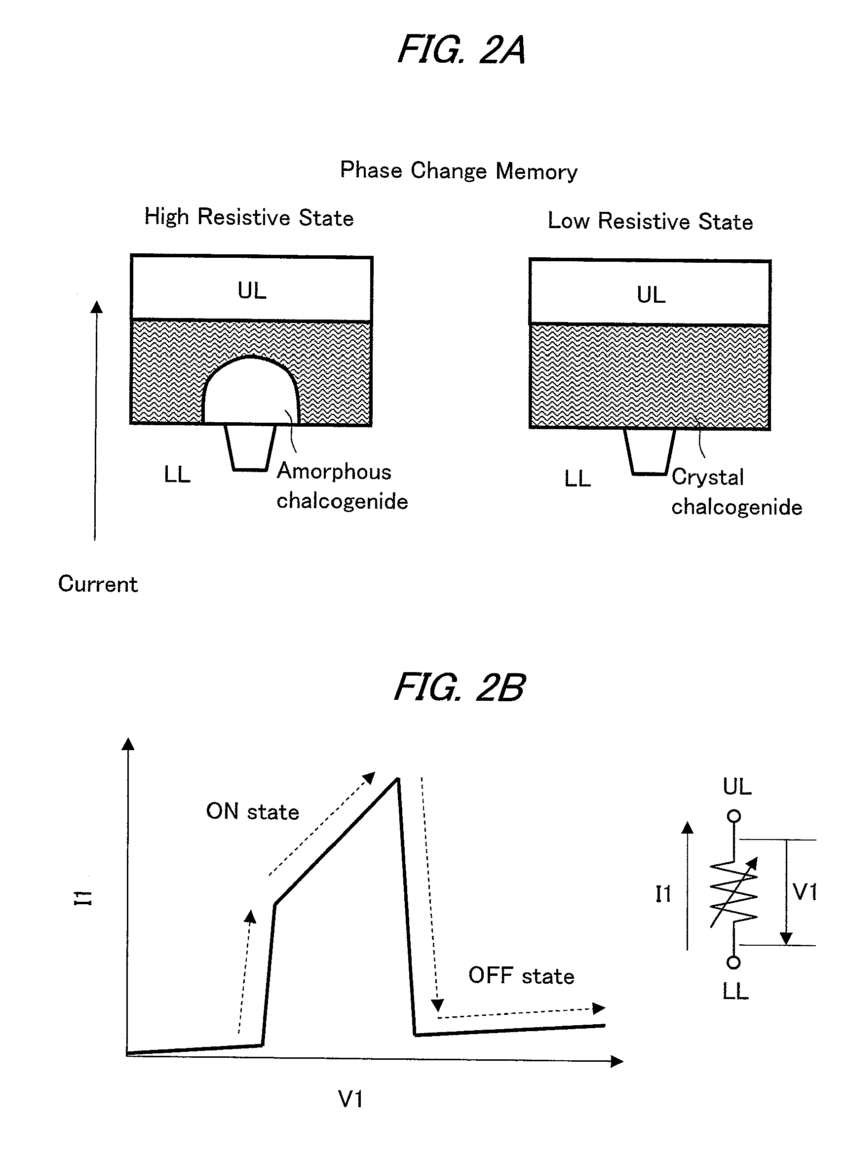
[0118]The thick line of FIG. 23 shows a path of the current flowing into the array when information of the memory cell MC disposed at the intersection of the word line WL0 and the local bit line LBL1 is rewritten (written) from, for example, a logical value “0” to “1”. When the connecting direction of a resistance change element is reversed, the rewriting from the logical value “1” to “0” can be performed with the same direction as the rewriting current shown in FIG. 23. A select element of the MC is constituted of, for example, one MOS transistor, and the source side is connected to a local source line LSL1 and the drain is connected to the resistance change element. As compared with the first embodiment, the ...

third embodiment

[0139]A semiconductor device according to a third embodiment will be described with reference to FIG. 30 to FIG. 35.

[0140]FIG. 30 shows one example of the operation of a memory cell array in the semiconductor device according to the third embodiment.

[0141]The thick line of FIG. 30 shows a path of the current flowing into the array when information of the memory cell MC disposed at the intersection of the word line WL511 and the local bit line LBL1 is rewritten (written) from, for example, a logical value “0” to “1”. When the connecting direction of a resistance change element is reversed, the rewriting from the logical value “1” to “0” can be performed with the same direction as the rewriting current shown in FIG. 30. A select element of the MC is constituted of, for example, one MOS transistor, and the source side is connected to a local source line LSL and the drain is connected to the resistance change element. A global bit line GBL0 is charged to a rewriting potential higher tha...


PUM


Abstract

A technique for increasing rewriting current without increasing a power supply voltage and also reducing location dependency inside a memory array of a resistive state after the rewriting is provided in a resistance change memory in which the resistance value of a memory cell changes between logical values “1” and “0”. In the resistance change memory, bit lines are formed into a layered structure, the bit line select switches for connecting to the global bit line are provided at both ends of the local bit line, and a control method of the bit line select switches is changed in the writing and the reading, thereby realizing the optimum array configurations for each of them. More specifically, in the writing and the reading, two current paths are provided in parallel by turning ON the bit line select switches simultaneously.

Description

CROSS-REFERENCE TO RELATED APPLICATION[0001]The present application claims priority from Japanese Patent Application No. JP 2008-120466 filed on May 2, 2008, the content of which is hereby incorporated by reference into this application.TECHNICAL FIELD OF THE INVENTION[0002]The present invention relates to a semiconductor device having a resistance change memory cell, and more particularly to a technique for realizing highly reliable reading and writing by reducing the parasitic resistance component and suppressing the variation of the resistance component in an array (hereinafter, referred to also as memory array and memory cell array).BACKGROUND OF THE INVENTION[0003]The scaling down of the manufacturing rule has been advanced in order to achieve higher integration in a dynamic random access memory (DRAM), but it has become difficult to manufacture a capacitor for providing sufficient signals. Thus, a resistance change memory cell in which a resistance change element is used in pl...

Claims


Application Information

Patent Timeline
Patent Type & Authority Patents(United States)
IPC IPC(8): G11C11/00
CPCG11C7/18G11C11/16G11C13/00G11C13/0004G11C13/0023G11C13/0026G11C13/0069G11C13/02G11C2013/0078G11C2213/79G11C11/1655G11C11/1659G11C11/1673G11C11/1675G11C11/15
Inventor ONO, KAZUOTAKEMURA, RIICHIROSEKIGUCHI, TOMONORI
Owner HITACHI LTD
Why Eureka
Try Eureka