Printed wiring board including a thermal land for supressing heat dissipation

a technology of printed wiring board and thermal land, which is applied in the direction of printed circuit details, circuit thermal arrangement, printed circuit, etc., can solve the problems of reducing connection reliability, adversely affecting connection reliability, and degrading of soldering finished condition, so as to reduce the heat capacity of through holes and suppress heat diffusion. , the effect of good finished condition

Inactive Publication Date: 2012-01-31
NEC CORP
View PDF18 Cites 5 Cited by
  • Summary
  • Abstract
  • Description
  • Claims
  • Application Information

AI Technical Summary

Benefits of technology

[0041]The present invention has been made in view of the above described circumstances, and its first objective is to provide a printed wiring board which can suppress thermal diffusion to maintain a good finished condition of soldering and thereby to ensure high connection reliability, and also to provide electronic equipment including the same printed wiring board that can accommodate trends towards an increase in the number of layers and use of a lead-free solder in the printed wiring board.

Problems solved by technology

When a high quality soldering cannot be achieved throughout within through holes 106a, 106b because of the above described reason, the connection strength becomes insufficient thereby adversely affecting connection reliability.
The first problem to be solved, according to the above described related arts is that, the temperature rise during soldering is still not sufficient and the finished condition of the soldering is degraded thereby reducing connection reliability.
That is, as the functionality of electronic equipment becomes increasingly sophisticated, the related thermal land technology cannot cope with the further increase in the number of layers of the multilayer printed wiring board, and the heat conduction path will be increased making it difficult to raise the temperature in the vicinity of a through hole.
Moreover, further increase in the thickness of the multilayer printed wiring board results in longer through holes making the soldering to the interior of the through hole more difficult.
Further, when a lead-free solder (for example, tin-silver-copper lead-free solder) is used due to a compulsory requirement, a problem arises in that the melting temperature increases by several tens of degrees.
Therefore, when a lead-free solder is used for soldering, since heating the soldering point up to 240 to 260 degrees C. is required, the ability of molten solder to rise tends to further decline making it difficult to achieve sound soldering.
Further, the second problem, according to the above described related arts is that, since current will flow in the spoke of the thermal land, such a narrow width portion will provide a high resistance thereby causing the current capacity to decline.
However, when the printed board is used after package components are mounted thereon via lead wires, current flows through a spoke which has a locally narrow width and a large resistance, causing heat to be generated.
This will lead to a decrease of current capacity and may cause the printed board to be burnt out.
Further, a third problem is that according to the above described related arts, signal transmission performance is degraded and the signal wiring density declines in signal wirings which are formed in the vicinity of through holes in the signal layers which are opposite to the power supply and ground layers formed with solid patterns via the insulation layer.
Because, in this portion, signal wiring 102f, 102g will have lost opposing ground layer 104, this will end up to cause disturbance in signal transmission.
This would cause a difference in electric properties between the pair wirings thus causing degradation of signal transmission performance.
Further, attempts to ensure enough clearance tend to result in a decrease in the wiring density of signal wiring.
Further, a fourth problem is that, according to the above described related arts, the evenness of the conductive layer in the vicinity of a through hole degrades.
This tends to cause degradation of the evenness of the conductive layer of a printed wiring board and variations of the property of the printed wiring board.

Method used


Image

  • Printed wiring board including a thermal land for supressing heat dissipation
  • Printed wiring board including a thermal land for supressing heat dissipation
  • Printed wiring board including a thermal land for supressing heat dissipation

Examples


exemplary embodiment 1

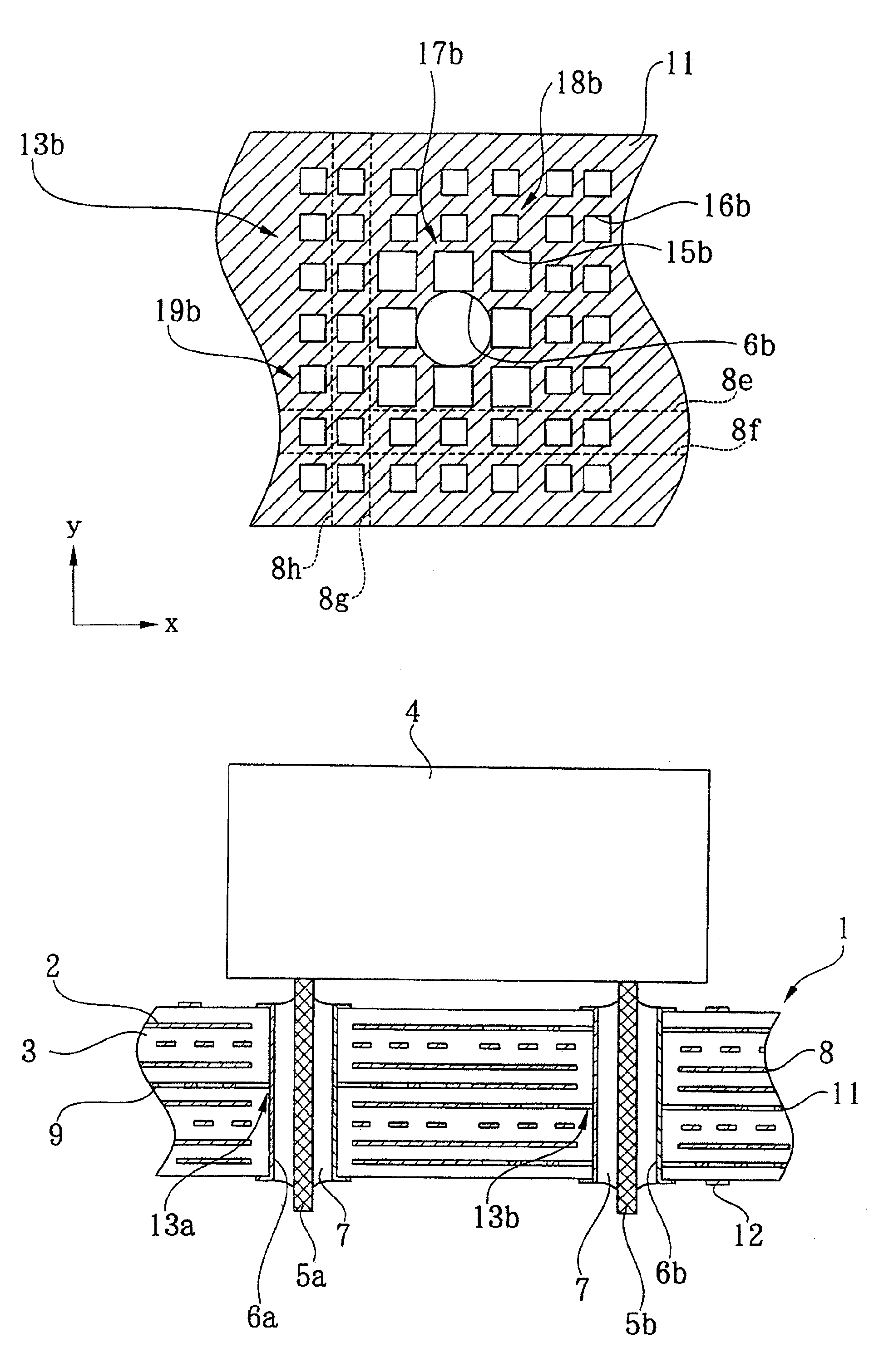
[0071]FIG. 4 is a sectional view showing the configuration of a thermal land formed in the ground layer of the multilayer printed wiring of board of a first exemplary embodiment. FIG. 5 is a sectional view showing the configuration of a thermal land formed in a power supply layer of the same multilayer printed wiring board. FIG. 6 is a sectional view to show the configuration of the same multilayer printed wiring board.

[0072]Multilayer printed wiring board 1 of this example is installed in electronic equipment such as computers and communication apparatuses, and has a multilayer structure in which a plurality of conductive layers 2 and insulation layers 3 are alternately laminated as shown in FIG. 6. Further, multilayer printed wiring board 1 includes a plurality of through holes 6a, 6b, . . . . The plurality of through holes 6a, 6b, . . . penetrate a plurality of conductive layers 2 and insulation layers 3 from the front face to the rear face, are inserted with lead wirings 5a, 5b,...

exemplary embodiment 2

[0119]FIG. 7 is a sectional view showing the configuration of the multilayer printed wiring board of a second exemplary embodiment.

[0120]The feature of the present exemplary embodiment that is different from the above described first exemplary embodiment is that it is applied to the mounting of surface mounted devices (SMD) in place of through-hole mounted devices.

[0121]Since the configurations other than the above are roughly the same as those of the above described first exemplary embodiment, in FIG. 7, the same components as those of the first exemplary embodiment are designated by using the same characters as used in FIG. 6, and the description thereof will be shortened.

[0122]Multilayer printed wiring board 1A of the present exemplary embodiment is installed in electronic equipment such as computers and communication apparatuses, and has a multilayer structure in which a plurality of conductive layers 21 and insulation layers 22 are alternately laminated as shown in FIG. 7. Furt...

exemplary embodiment 3

[0132]FIG. 8 is a sectional view showing the configuration of the multilayer printed wiring board of a third exemplary embodiment.

[0133]The feature of the present exemplary embodiment is that significantly different from the second exemplary embodiment is that multilayer printed wiring board 1A is configured to be a built-up substrate.

[0134]Since the configurations other than the above are roughly the same as those of the above described second exemplary embodiment, in FIG. 8, the same components as those of the second exemplary embodiment are designated by using the same characters as used in FIG. 7, and the description thereof will be shortened.

[0135]Multilayer printed wiring board 1B of the present exemplary embodiment is installed in electronic equipment such as computers and communication apparatuses. Multilayer printed wiring board 1B is made up of core layer 43 and a built-up substrate as shown in FIG. 8. Core layer 43 is a multilayer structure in which a plurality of conduct...


PUM


Abstract

When soldering is performed, heat transferred from through hole 6b is caused to bypass a mesh-like copper foil region between non-copper-foil regions and thus the transfer of heat to a solid pattern region around thermal land 13b is delayed. Signal wirings 8e, 8f and signal wirings 8g, 8 are formed along the arrangement directions of non-copper-foil regions 15b, 16b respectively keeping a predetermined spacing between them and disposed to overlap copper foil regions, thus ensuring a current return path by means of opposing ground layer 11.

Description

INCORPORATION BY REFERENCE[0001]This application is the National Phase of PCT / JP2007 / 064852, filed Jul. 30, 2007, which claims priority to Japanese Patent Application No. 2006-211450, filed on Aug. 2, 2006, which is incorporated herein by reference in its entirety.TECHNICAL FIELD[0002]The present invention relates to a printed wiring board and electronic equipment comprising the printed wiring board, and for example relates to a printed wiring board in which a thermal land for suppressing heat dissipation is formed around a through hole of a solid pattern, and electronic equipment comprising the printed wiring board.BACKGROUND ART[0003]Electronic equipment such as computer apparatuses and communication apparatuses is generally configured to be installed with a printed wiring board, on which components such as through-hole mounted devices are mounted. Through-hole mounted devices are connected to desired conductive layers in the printed wiring board in such a way that a lead wire for...

Claims


Application Information

Patent Timeline
Patent Type & Authority Patents(United States)
IPC IPC(8): H05K1/00
CPCH05K1/0201H05K1/116H05K3/3447H05K3/3494H05K1/114H05K3/3436H05K3/429H05K2201/062H05K2201/09681H05K2201/0969H05K2201/10734
Inventor ISHIDA, HISASHI
Owner NEC CORP
Why Eureka
Try Eureka