Load calculation control method and apparatus
a load calculation and control method technology, applied in the direction of process and machine control, ignition automatic control, instruments, etc., can solve the problems of electrode water freezing under a below-zero environment during wintertime, electrode water temperature rise, etc., to achieve more accurate load control value setting, continuous and very accurate load adjustment, and shorten the effect of tim
- Summary
- Abstract
- Description
- Claims
- Application Information
AI Technical Summary
Benefits of technology
Problems solved by technology
Method used
Image
Examples
embodiments 1
[0085]In the following, embodiments 1 and 2 of the invention using the foregoing apparatus example and method example are described with reference to the one-line wiring diagrams in FIGS. 6-8.
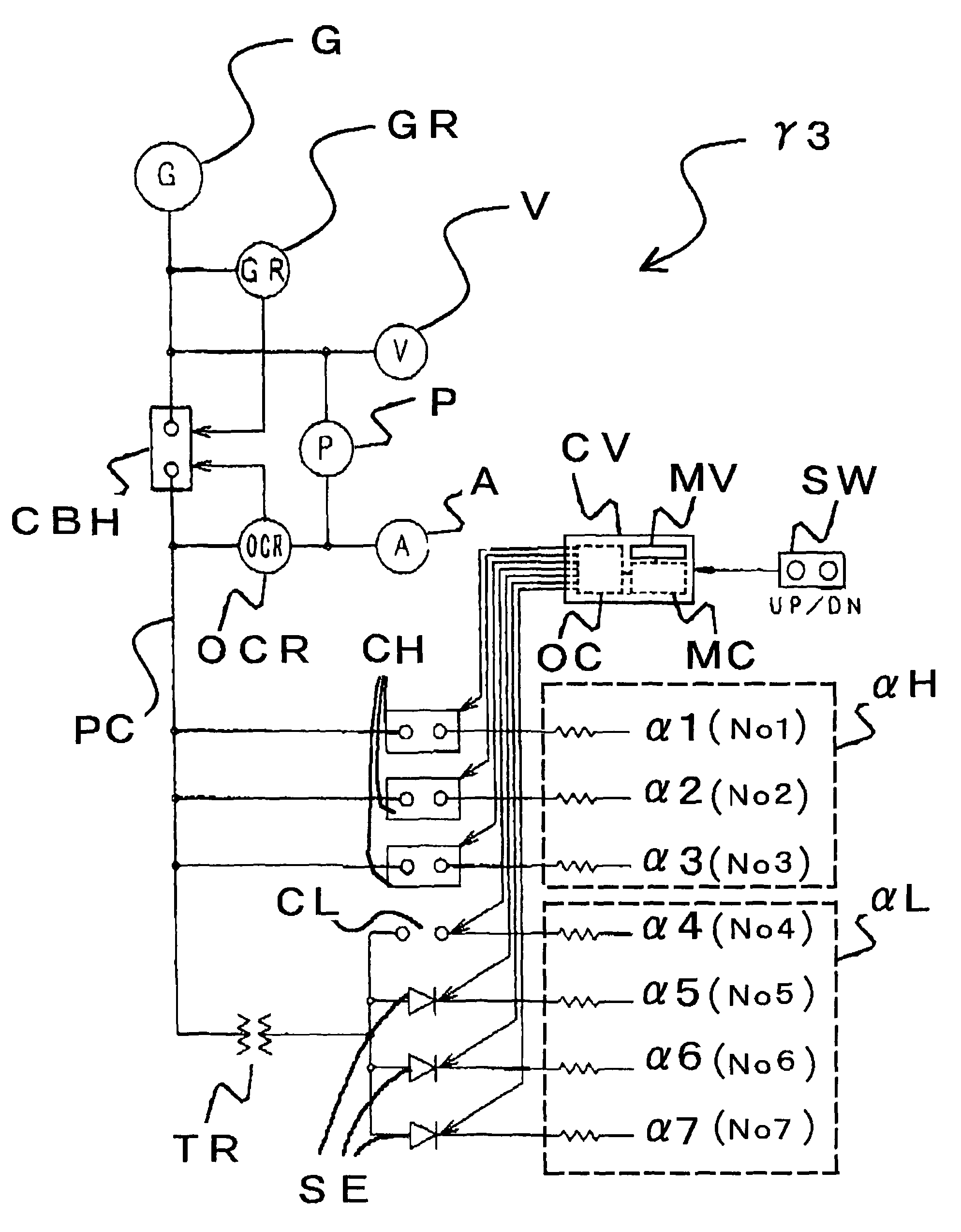
[0086]First, the structure of a high-voltage load device γ2 will be described in connection with FIG. 6, wherein combined application of a high-voltage bank αH and a low-voltage bank αL is enabled by connecting the high-voltage load device γ2 to the aforementioned high-voltage load device γ1 shown in FIG. 3 via the controller CV and the push button switch SW and to the power cable PC via the transformer TR.
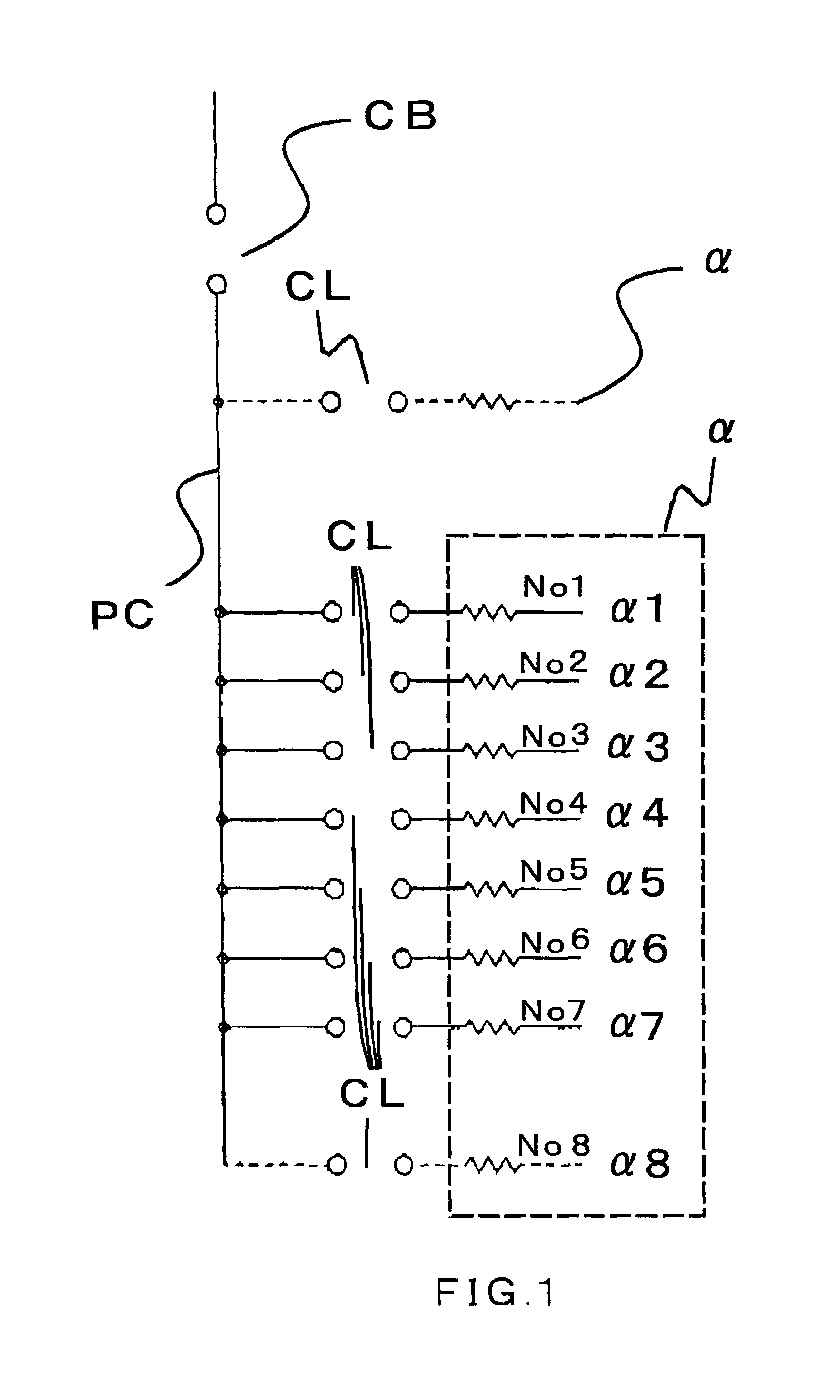
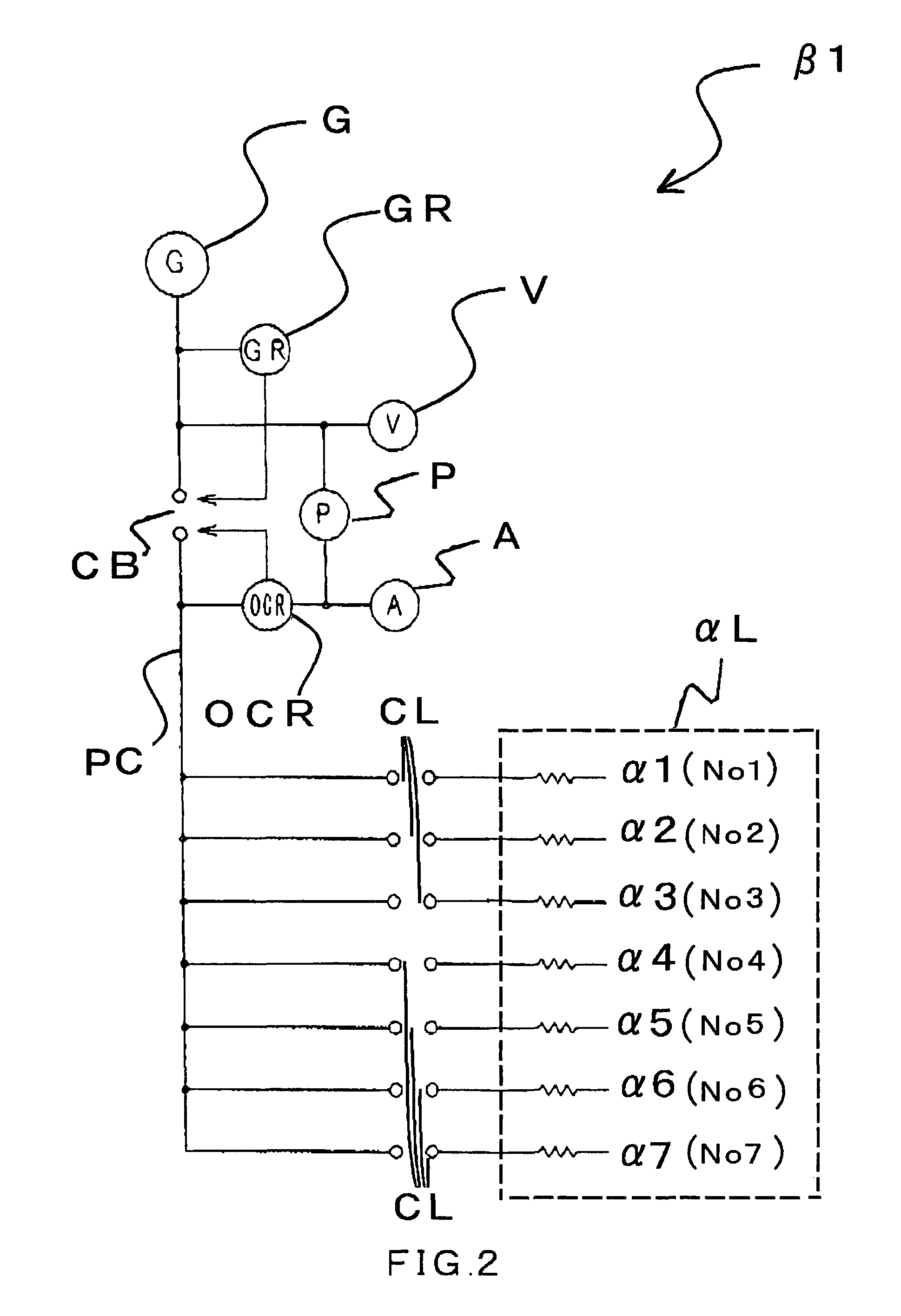
[0087]For a high-voltage load device wherein a load control value is set by the use of a controller CV by dividing a resistor bank into seven based on a geometric progression by multiplying first the load control value and then the previous one by the common ration 0.5 similar to the conventional load devices, continuous load adjustments are possible. However, when a step turning the switch t...
embodiments 2
[0091]In the following, an embodiment of a load device using a semiconductor switch will be described with reference to FIGS. 7 and 8.
[0092]Load adjustments near a load control value, radiant heat from other resistor banks, switching, and fine adjustments of load depending on an outside air temperature considerably deteriorates the resistor banks of small capacity. Therefore, the workload of the resistor banks α5-α7 having a small capacity is reduced and a semiconductor switch SE is used together
[0093]FIG. 7 shows a one-line wiring diagram of the low-voltage load device β3 to which semiconductor switches are added. Connecting small-capacity resistor banks α5-α7 of high switching frequency via such semiconductor switches SE would result in maintaining the contact life of the switch.
[0094]On the other hand, FIG. 8 is a one-line wiring diagram of the high-voltage load device β3 to which semiconductor switches are added. Specifically, such semiconductor switches are added to the high-vo...
PUM
 Abstract
Description
Claims
Application Information


