High light extraction efficiency nitride based light emitting diode by surface roughening

a technology of light-emitting diodes and gallium nitride, which is applied in the direction of basic electric elements, electrical equipment, semiconductor devices, etc., can solve the problems of little room for improvement over these values, difficult to increase internal quantum efficiency, and crystal quality and epitaxial layer structure, etc., to achieve increased incidence angles, small refractive index, and increased chance

Active Publication Date: 2012-02-14
RGT UNIV OF CALIFORNIA
View PDF15 Cites 17 Cited by
  • Summary
  • Abstract
  • Description
  • Claims
  • Application Information

AI Technical Summary

Benefits of technology

[0015]The present invention describes a method of increasing the light extraction efficiency from a nitride based LED, which involves photolithography and plasma-assisted chemical dry etching. Through increasing light extraction, subsequent improvement of efficiency is thus expected. One most noticeable advantage of the present invention is that it significantly increases the light extraction efficiency from a nitride-based LED, including films that are grown along nonpolar and semipolar orientations. In addition, this invention is more straightforward compared to other light extraction enhancement techniques, such as using a photonic crystal. More important, unlike photo-enhanced chemical etching that is also a simple light extraction enhancement technique, the present invention is more versatile as it could be applied to any nitride semiconductor surface regardless of its crystal structure.
[0016]Therefore, to overcome the limitations in the prior art described above, and to overcome other limitations that will become apparent upon reading and understanding the present specification, the present invention describes a method for fabricating a III-nitride LED, comprising texturing at least one surface of a semipolar or nonpolar plane of a III-nitride layer of the LED to form a textured surface, wherein the texturing step is performed by plasma assisted chemical etching. The texturing step may be performed by photolithography followed by the etching, or the textured surface may be formed using nano-imprinting followed by the etching. Light emitted by an active region of the LED is mostly extracted from the textured surface.
[0017]The texturing step may further comprise: (1) creating at least one feature with at least one sidewall that reflects and transmits at least one light ray incident from inside the feature; and inclining the sidewall such that each time the ray is reflected, an angle of incidence of the ray relative to a surface normal of the sidewall decreases, such that when the angle of incidence of the ray is smaller than a critical angle, the ray's transmission through the sidewall is increased, and when the angle of incidence of the ray is at least equal to the critical angle, the ray is reflected by the sidewall.
[0018]The present invention further discloses a method for emitting light from a III-nitride LED, comprising emitting the light from at least one textured surface of a semipolar or nonpolar plane of a III-nitride layer of the LED, wherein the texturing is performed by plasma assisted chemical etching.
[0019]The present invention further discloses a III-nitride LED, comprising n-type III-nitride; p-type III-nitride; a III-nitride active layer, that emits light, formed between the n-type III-nitride and p-type III-nitride; a III-nitride light extraction surface on the n-type III-nitride and forming an interface with an external medium, wherein the III-nitride light extraction surface has features with at least one sloped sidewall which transmits the light into external medium air at the interface and reflects the light at the interface, wherein: (1) the reflected light, after undergoing subsequent reflections inside the features, has an increased incidence angle relative to the interface and consequently an increased chance of being transmitted to the external medium, and (2) the n-type III-nitride, p-type III-nitride, and III-nitride active layer are semi-polar or non-polar layers. The external medium may be a medium with a smaller refractive index than III-nitride, for example air or a vacuum.

Problems solved by technology

Increasing the internal quantum efficiency, determined by crystal quality and epitaxial layer structure, could be rather difficult.
There might be little room for improvement over these values, especially for nonpolar and semipolar oriented devices grown on high quality freestanding GaN substrates.

Method used


Image

  • High light extraction efficiency nitride based light emitting diode by surface roughening
  • High light extraction efficiency nitride based light emitting diode by surface roughening
  • High light extraction efficiency nitride based light emitting diode by surface roughening

Examples


Embodiment Construction

[0033]In the following description of the preferred embodiment, reference is made to the accompanying drawings which form a part hereof, and in which is shown by way of illustration a specific embodiment in which the invention may be practiced. It is to be understood that other embodiments may be utilized and structural changes may be made without departing from the scope of the present invention.

TECHNICAL DESCRIPTION

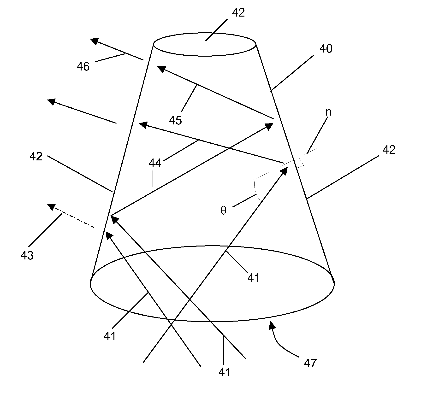
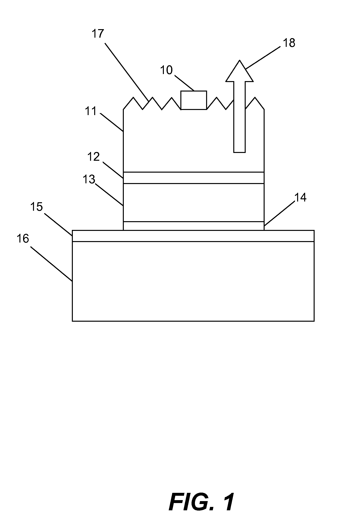
[0034]The present invention describes a technique for increasing the light extraction efficiency from a nitride based LED, which involves photolithography and plasma-assisted chemical dry etching. Through increasing light extraction, subsequent improvement of efficiency is thus expected.

[0035]In one embodiment of the present invention, the freestanding GaN substrate surface of the opposite side of the LED growth front is roughened. After the device is fabricated, the LED is then placed within a shaped optical element.

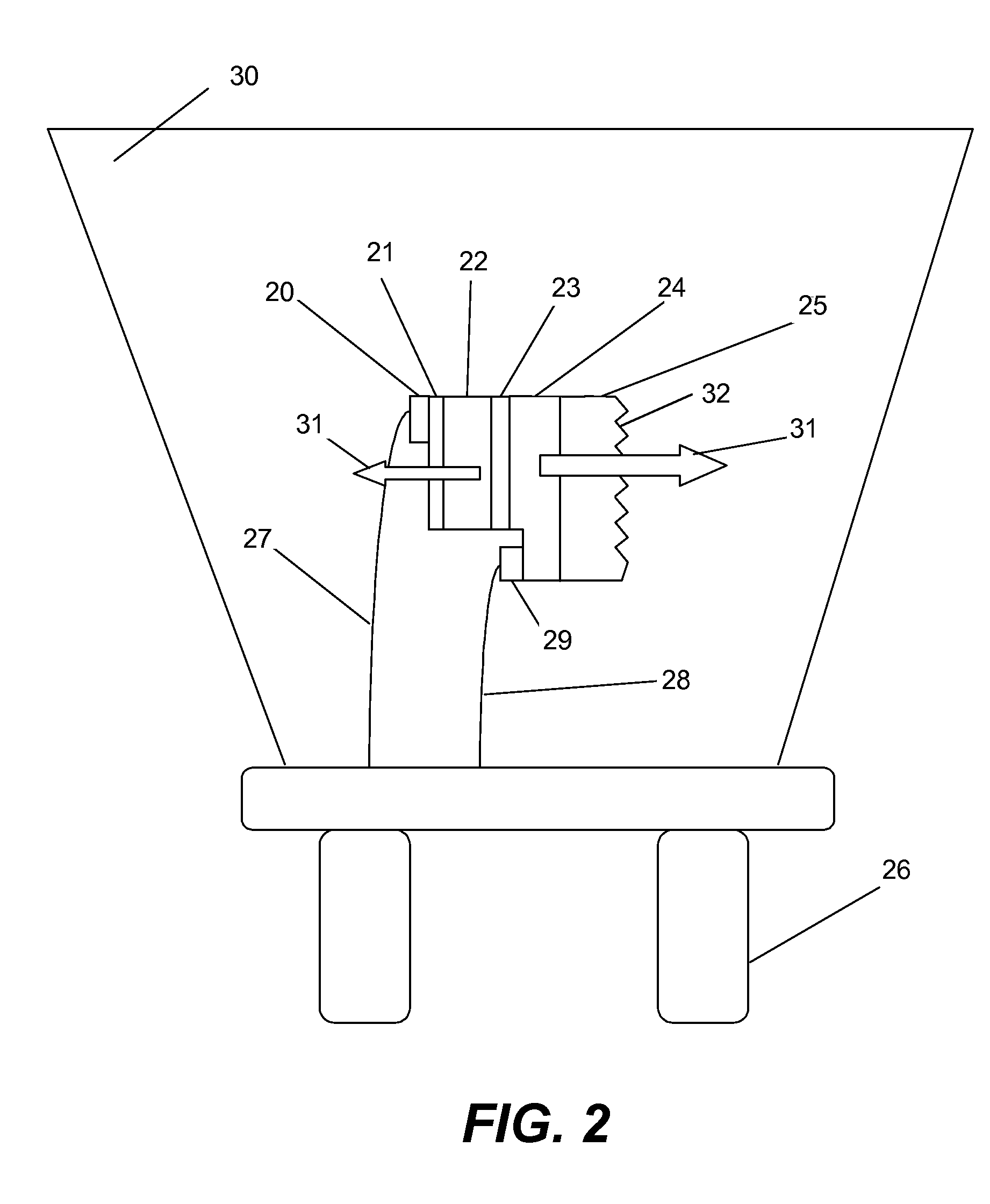
[0036]FIG. 2 shows a schematic representation of a su...


PUM


Abstract

A III-nitride light emitting diode (LED) and method of fabricating the same, wherein at least one surface of a semipolar or nonpolar plane of a III-nitride layer of the LED is textured, thereby forming a textured surface in order to increase light extraction. The texturing may be performed by plasma assisted chemical etching, photolithography followed by etching, or nano-imprinting followed by etching.

Description

CROSS REFERENCE TO RELATED APPLICATION[0001]This application claims the benefit under 35 U.S.C. Section 119(e) of co-pending and commonly-assigned U.S. Provisional Patent Application Ser. No. 60 / 991,617, filed on Nov. 30, 2007, by Hong Zhong, Anurag Tyagi, Kenneth J. Vampola, James S. Speck, Steven P. DenBaars, and Shuji Nakamura, entitled “HIGH LIGHT EXTRACTION EFFICIENCY NITRIDE BASED LIGHT EMITTING DIODE BY SURFACE ROUGHENING,” which application is incorporated by reference herein.BACKGROUND OF THE INVENTION[0002]1. Field of the Invention[0003]This invention relates to light emitting diodes (LEDs) and more particularly to high light extraction efficiency gallium nitride based LEDs via surface roughening.[0004]2. Description of the Related Art[0005](Note: This application references a number of different publications as indicated throughout the specification by one or more reference numbers within brackets, e.g., [x]. A list of these different publications ordered according to the...

Claims


Application Information

Patent Timeline
Patent Type & Authority Patents(United States)
IPC IPC(8): H01L21/00H01L33/20H01L33/22H01L33/32
CPCH01L33/22H01L33/32H01L21/02433H01L33/0075H01L33/10H01L21/02458H01L33/20H01L33/18H01L2933/0083
Inventor ZHONG, HONGTYAGI, ANURAGVAMPOLA, KENNETH J.SPECK, JAMES S.DENBAARS, STEVEN P.NAKAMURA, SHUJI
Owner RGT UNIV OF CALIFORNIA
Why Eureka
Try Eureka