Short-channel silicon carbide power mosfet

a technology of silicon carbide and power mosfet, which is applied in the direction of semiconductor devices, electrical equipment, basic electric elements, etc., can solve the problems of high specific on-resistance, and achieve the effect of increasing on-state current density and reducing specific on-resistan

Active Publication Date: 2012-03-13
PURDUE RES FOUND INC
View PDF27 Cites 12 Cited by
  • Summary
  • Abstract
  • Description
  • Claims
  • Application Information

AI Technical Summary

Benefits of technology

[0008]The present invention provides high voltage power MOSFETs in silicon carbide that have channel lengths considerably shorter than possible with conventional techniques, and thereby provides reduced specific on-re

Problems solved by technology

However, 4H-SiC MOSFETs suffer from low inversion chan

Method used


Image

  • Short-channel silicon carbide power mosfet
  • Short-channel silicon carbide power mosfet
  • Short-channel silicon carbide power mosfet

Examples


Embodiment Construction

[0017]For the purpose of promoting an understanding of the principles of the invention, reference will now be made to the embodiments illustrated in the drawings and specific language will be used to describe the same. It will nevertheless be understood that no limitation of the scope of the invention is thereby intended, such alterations and further modifications in the illustrated device and such further applications of the principles of the invention as illustrated therein being contemplated as would normally occur to one skilled in the art to which the invention relates.

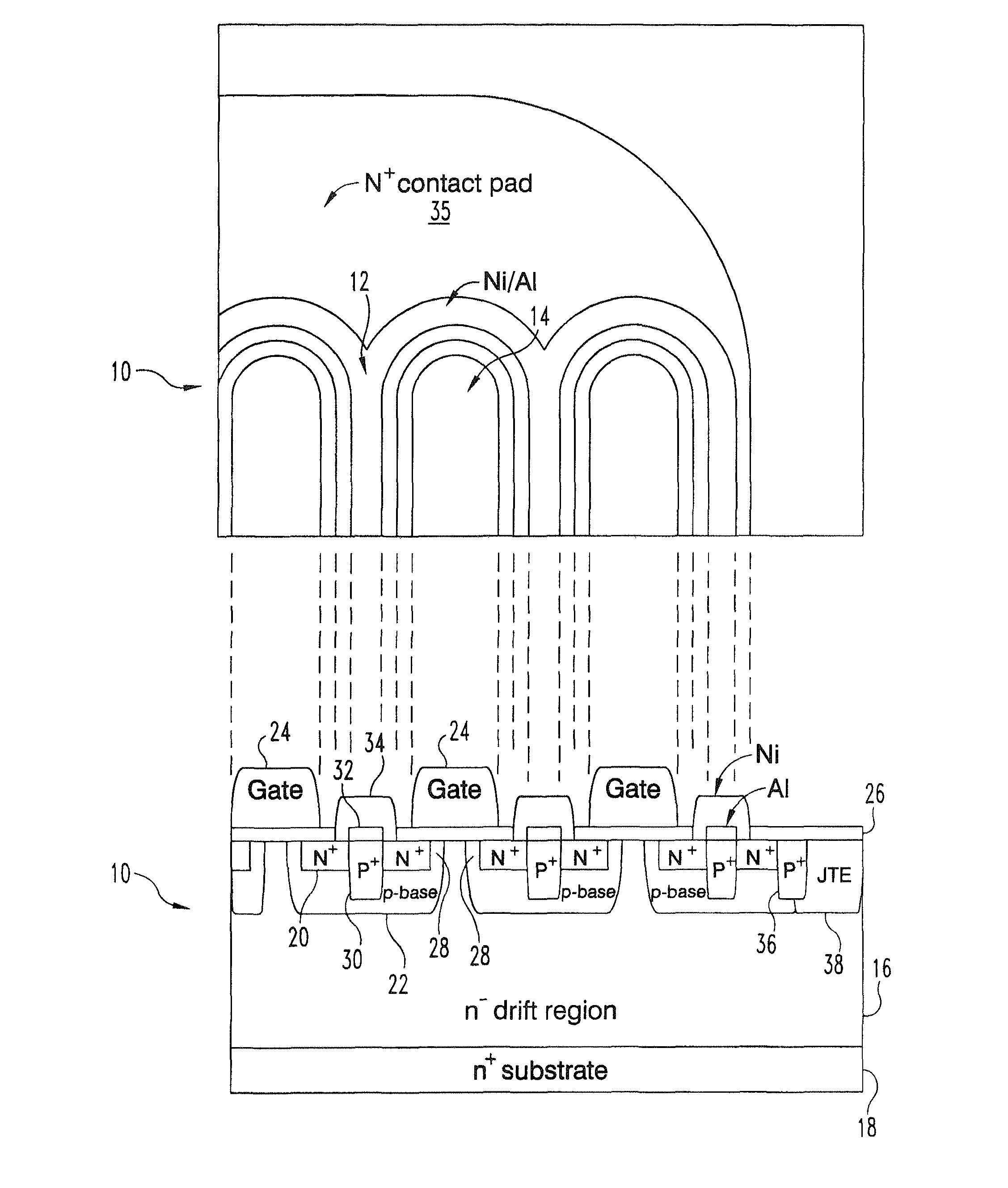
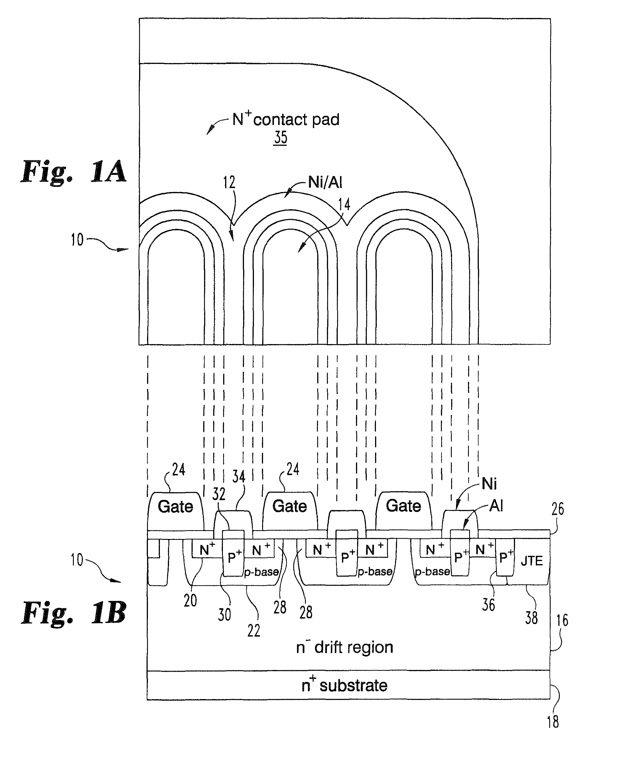
[0018]The channel length, Lch, which is the distance between the source and drift regions at the interface between the semiconductor and the gate oxide, is lithographically defined in a SiC DMOSFET by ion implantations of the source and base regions. This limits the minimum channel length due to a required alignment tolerance between the base and source implant masks during the photolithography process. The prese...


PUM


Abstract

A silicon carbide power MOSFET having a drain region of a first conductivity type, a base region of a second conductivity type above the drain region, and a source region of the first conductivity type adjacent an upper surface of the base region, the base region including a channel extending from the source region through the base region adjacent a gate interface surface thereof, the channel having a length less than approximately 0.6 μm, and the base region having a doping concentration of the second conductivity type sufficiently high that the potential barrier at the source end of the channel is not lowered by the voltage applied to the drain. The MOSFET includes self-aligned base and source regions as well as self-aligned ohmic contacts to the base and source regions.

Description

CROSS-REFERENCE TO RELATED APPLICATION[0001]This application is a divisional of patent application Ser. No. 10 / 821,613, filed Apr. 9, 2004, and claims the benefit of Provisional Patent Application. No. 60 / 462,127, filed Apr. 11, 2003, both of which applications are hereby incorporated by reference along with all references cited therein.GOVERNMENT RIGHTS[0002]This invention was made with government support under Contract / Grant No. N00014-01-1-0072 awarded by the Office of Naval Research. The government has certain rights in the invention.BACKGROUND OF THE INVENTION[0003]The present invention relates to power semiconductor devices, and more particularly to power MOSFETs formed in silicon carbide (SiC).[0004]Power MOSFETs are well known for their ability to carry large currents in the on-state while withstanding large breakdown voltages in the off-state. In such a device, current flow between source and drain regions in a semiconductor substrate is controlled by a voltage applied to a...

Claims


Application Information

Patent Timeline
IPC IPC(8): H01L21/336
CPCH01L21/046H01L21/0475H01L29/66068H01L29/7802Y10S438/931H01L29/7811
Inventor COOPER, JAMES A.MATIN, MAHERIN
Owner PURDUE RES FOUND INC
Why Eureka
Try Eureka