Ultra-high-speed large-current longitudinal insulated gate bipolar transistor

A bipolar transistor, high current technology, applied in the direction of circuits, electrical components, semiconductor devices, etc., can solve the problems that have not completely solved the conduction performance and switching performance of power semiconductor devices, and other performance reduction of devices

Pending Publication Date: 2019-12-27
UNIV OF ELECTRONIC SCI & TECH OF CHINA
View PDF15 Cites 0 Cited by
  • Summary
  • Abstract
  • Description
  • Claims
  • Application Information

AI Technical Summary

Problems solved by technology

[0004] These solutions can improve the performance of the Gemini conductive power semiconductor device to a certain extent, but in the case of improving a certain performance of the device, other performances of the device are also reduced, and have not completely solved the conduction performance and switching performance of the power semiconductor device. the contradiction between

Method used


Image

  • Ultra-high-speed large-current longitudinal insulated gate bipolar transistor
  • Ultra-high-speed large-current longitudinal insulated gate bipolar transistor
  • Ultra-high-speed large-current longitudinal insulated gate bipolar transistor

Examples


Embodiment 1

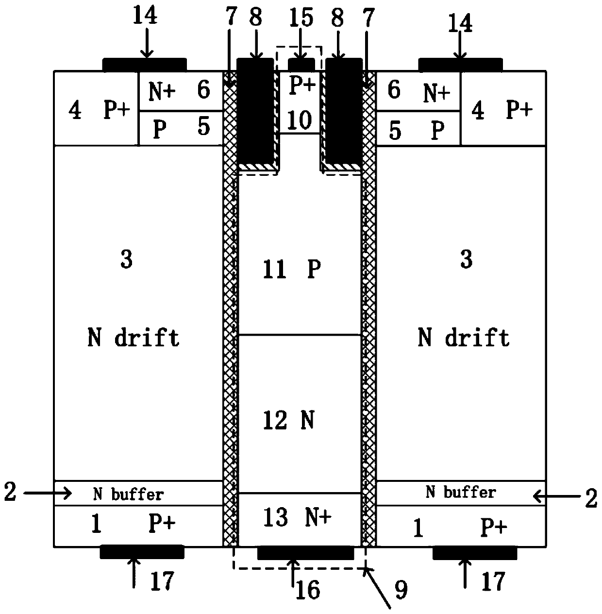
[0025] See attached figure 1 . This embodiment is a vertical insulated gate bipolar transistor, the main structure includes collector (1), buffer zone (2), drift zone (3), ohmic contact heavily doped zone (4), channel zone (5) , emitter (6), insulating dielectric layer (7), main grid (8), electric field strengthening unit (9); the electric field strengthening unit (9) is embedded in the middle of the device, including grounding electrode (10), P-type doped Region (11), N-type doped region (12), slave gate (13), ground electrode lead-out line (15), and gate lead-out line (16). Wherein, the material of the ground electrode (10), the P-type doped region (11), the N-type doped region (12), and the slave gate (13) can be silicon or polysilicon. The insulating medium layer (7) used to isolate the electric field strengthening unit (9) from other regions can be a conventional insulating medium, such as silicon dioxide, or a high dielectric constant medium, such as hafnium dioxide. ...

Embodiment 2

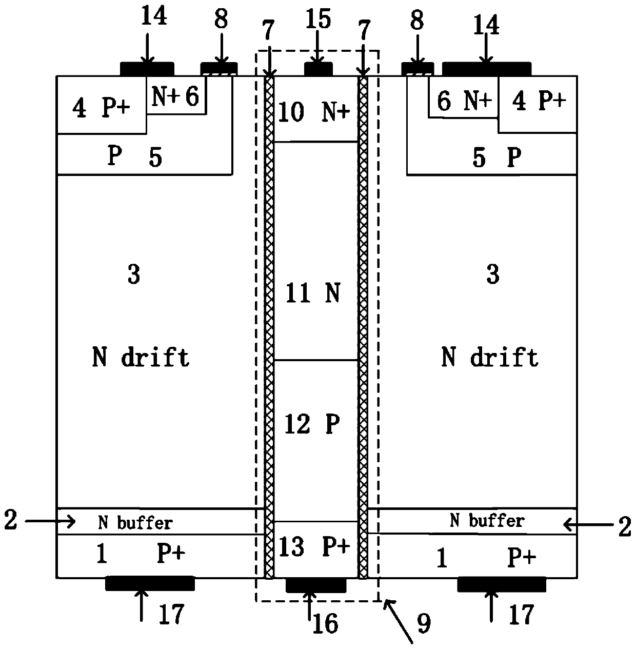
[0031] See attached figure 2 . This embodiment is a vertical insulated gate bipolar transistor, which mainly includes a collector (1), a buffer zone (2), a drift zone (3), an ohmic contact heavily doped zone (4), a channel zone (5), Emitter (6), insulating dielectric layer (7), main grid (8), electric field strengthening unit (9); the electric field strengthening unit (9) is located in the middle of the device, including grounding electrode (10), P-type doped region ( 11), N-type doped region (12), from gate (13), lead-out line from ground electrode (15), lead-out line from gate (16). Wherein, the material of the ground electrode (10), the P-type doped region (11), the N-type doped region (12), and the slave gate (13) can be silicon or polysilicon. The insulating medium layer (7) used to isolate the electric field strengthening unit (9) from other regions can be a conventional insulating medium, such as silicon dioxide, or a high dielectric constant medium, such as hafnium ...

Embodiment 3

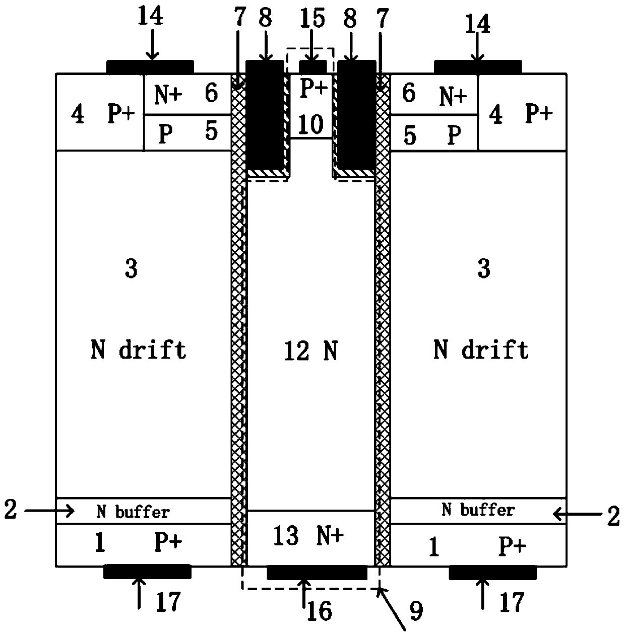
[0035] See attached image 3 . This embodiment is a vertical insulated gate bipolar transistor, the main structure includes collector (1), buffer zone (2), drift zone (3), ohmic contact heavily doped zone (4), channel zone (5) , emitter (6), insulating dielectric layer (7), main gate (8), electric field strengthening unit (9); the electric field strengthening unit (9) is embedded in the middle of the device, including grounding electrode (10), N-type doped The area (12), the grid (13), the ground electrode lead-out line (15), and the grid lead-out line (16). Wherein, the materials of the ground electrode (10), the N-type doped region (12) and the slave gate (13) can be selected from silicon or polysilicon. The insulating medium layer (7) used to isolate the electric field strengthening unit (9) from other regions can be a conventional insulating medium, such as silicon dioxide, or a high dielectric constant medium, such as hafnium dioxide. The use of conventional insulating...


PUM


Abstract

The invention discloses an ultra-high-speed large-current longitudinal insulated gate bipolar transistor and belongs to the field of power semiconductor devices. The ultra-high-speed large-current longitudinal insulated gate bipolar transistor comprises a collector, a buffer region, a drift region, an ohmic contact heavily doped region, a channel region, an emission region, an insulating dielectric layer and a main grid. The transistor is characterized in that an electric field strengthening unit is arranged in the middle of the transistor; the electric field strengthening unit is used for generating an electric field pointing to the electric field strengthening unit from the collector; and the electric field strengthening unit is isolated from the other parts of the transistor through aninsulating dielectric. The on-state current density of the device can be increased; an electric field modulation effect in the drift region can be enhanced; the resistance of the drift region of the device is reduced; on-state voltage drop is reduced; and the electric field can accelerate the removal of excess carriers in the drift region when the device is about to be turned off, so that the turn-off time of the device is greatly shortened, and a trailing current phenomenon is inhibited.

Description

technical field [0001] The present invention relates to power semiconductor devices. Background technique [0002] An ideal power device should have such characteristics: in forward conduction mode, it can pass any amount of current under zero conduction voltage drop; in reverse blocking mode, it can maintain any voltage under zero leakage current. Further, an ideal power device should be able to switch between on-state and off-state with zero switching time. However, actual power devices cannot achieve such characteristics. In power semiconductor devices, switching performance and conduction performance have always been a contradictory relationship. Gemini conduction power semiconductor devices, such as IGBT, in the case of a large conduction current, the number of carriers involved in conduction is large, which will inevitably lead to a large amount of charge stored in the drift region, which means that when the device needs to be turned off , it takes a long time to rem...

Claims


Application Information

Patent Timeline
IPC IPC(8): H01L29/739H01L29/06
CPCH01L29/7395H01L29/0619
Inventor 李俊宏刘奎方胡斌
Owner UNIV OF ELECTRONIC SCI & TECH OF CHINA
Why Eureka
Try Eureka