A lateral MOSFET device and a method for fabricate that same

A device and lateral technology, applied in the field of power semiconductors, can solve the problems of poor reliability, poor reverse recovery characteristics, and high power loss, achieve good shielding effect, reduce the electric field level, and improve the electric field concentration effect.

Active Publication Date: 2019-01-11
UNIV OF ELECTRONICS SCI & TECH OF CHINA
View PDF6 Cites 1 Cited by
  • Summary
  • Abstract
  • Description
  • Claims
  • Application Information

AI Technical Summary

Problems solved by technology

[0006] The present invention provides a lateral MOSFET device for the problems of poor long-term application reliability caused by excessively high gate dielectric layer e...

Method used


Image

  • A lateral MOSFET device and a method for fabricate that same
  • A lateral MOSFET device and a method for fabricate that same
  • A lateral MOSFET device and a method for fabricate that same

Examples


Embodiment 1

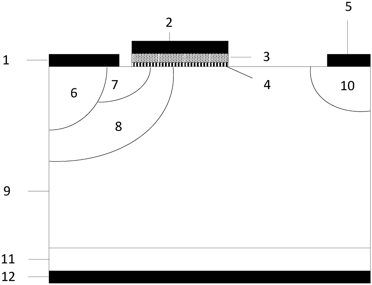
[0098] In a lateral silicon carbide MOSFET provided in this embodiment, the device cell structure is as follows: figure 2 As shown, it includes a substrate electrode 12, a P-type silicon carbide substrate 11 and a silicon carbide N- epitaxial layer 9 stacked vertically from bottom to top, and the top layer on one side of the N-type silicon carbide epitaxial layer 9 is provided with silicon carbide N type drain region 10, the top layer on the other side is provided with a silicon carbide N+ source region 7; the upper surface of the silicon carbide N-type drain region 10 is provided with a drain metal 5; it is characterized in that: the silicon carbide N- epitaxial layer 9 The top layer is also provided with a polysilicon region 13; the polysilicon region 13 is adjacent to the silicon carbide N+ source region 7 and is arranged on the side away from the drain metal 5; the upper surface of the polysilicon region 13 and part of the silicon carbide N+ source region 7 The upper surf...

Embodiment 2

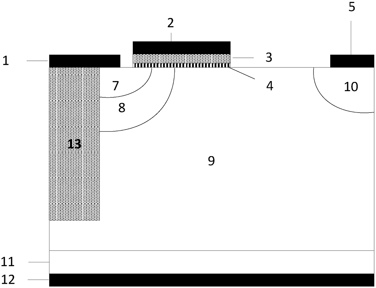
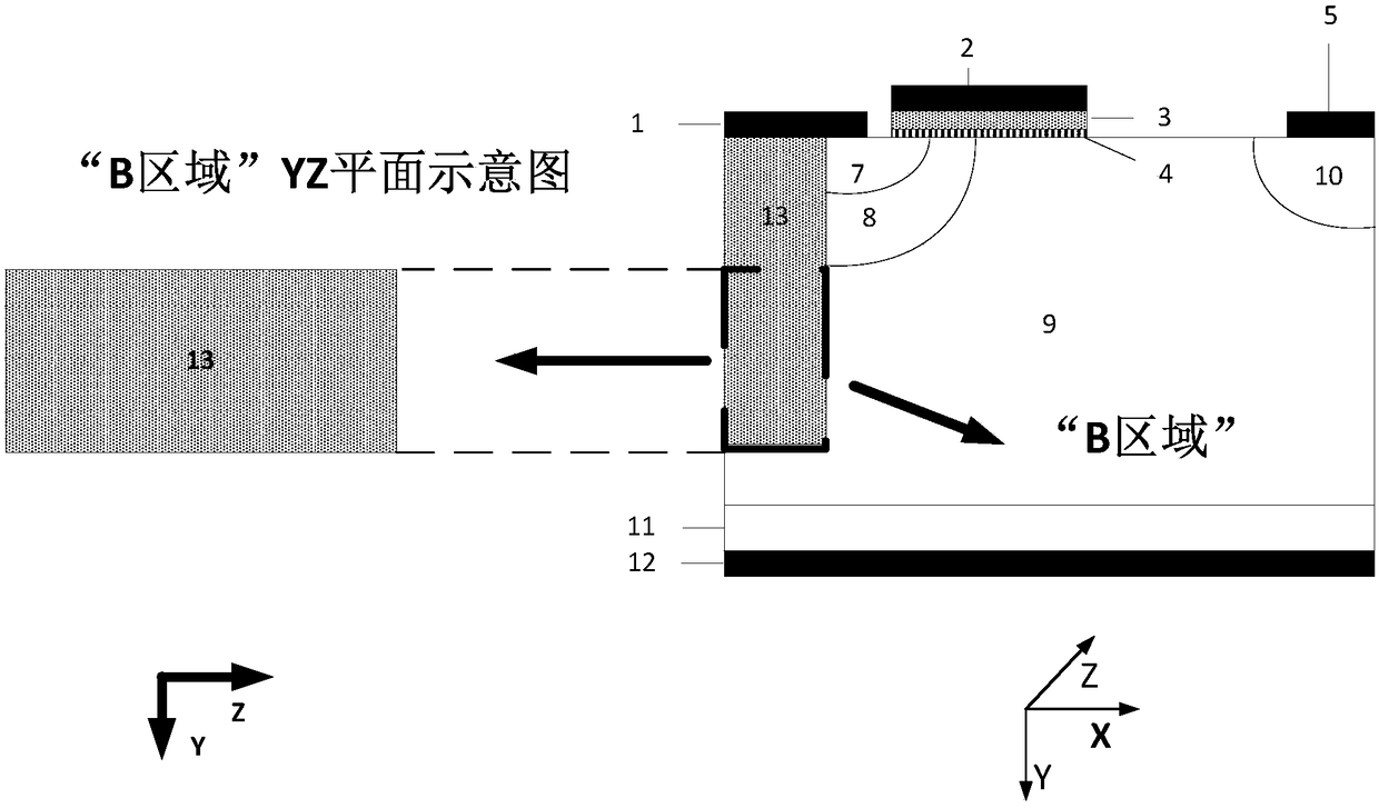
[0101] A lateral silicon carbide MOSFET provided in this embodiment, the cell structure of the device in this embodiment is as follows Figure 4 As shown, it differs from Embodiment 1 in that the bottom layer of the polysilicon region 13 of the present invention is set as independent polysilicon partitions, and several narrow-bandgap semiconductor partitions are isolated by the N- epitaxial layer 9 . like Figure 4 Shown in the "Area B" area. The conventional design of embodiment 1 same area is as image 3 shown. In this embodiment, the contact area between the integrated diode device and the silicon carbide N-epitaxy 9 is increased, so as to have better on-state performance of the diode.

Embodiment 3

[0103] A lateral silicon carbide MOSFET provided in this embodiment, the cell structure of the device in this embodiment is as follows Image 6 As shown, it differs from Embodiment 1 in that the lateral silicon carbide MOSFET device also has a three-dimensional gate structure, such as Image 6 Shown in area C. The three-dimensional gate structure increases the channel area of ​​the device during forward conduction, thereby optimizing the forward performance of the MOSFET;


PUM

PropertyMeasurementUnit
Thicknessaaaaaaaaaa
Thicknessaaaaaaaaaa
Thicknessaaaaaaaaaa

Abstract

A lateral MOSFET device belongs to that technical field of power semiconductor device. According to the invention, by trench filling, the contact region and the lower portion of the conventional lateral MOSFET device structure are replaced by polysilicon regions or Schottky contact metal regions so as to form a heterojunction or Schottky contact with rectifying characteristics. Since the heterojunction or Schottky contact is a multi-child device and the conduction voltage drop is lower than that of a conventional parasitic diode, the reverse recovery characteristics of the device can be optimized and excellent third-quadrant on-state performance can be achieved; Compared with the external anti-shunt diode, the external anti-shunt diode significantly reduces the volume of the electronic power system, reduces the packaging cost, reduces the parasitic effect of the interconnect and the interconnect, and improves the reliability of the system. At that same time, the problem that the electric field of the gate dielectric is too high is optimize, so that the reliability of the device can be improved for a long time. In addition, the preparation method of the device is simple and controllable, easy to realize, and promotes the popularization of the semiconductor power device in numerous practical applications.

Description

technical field [0001] The invention belongs to the technical field of power semiconductors, and in particular relates to a Lateral-Metal Oxide Semiconductor Field Effect Transistor, a Lateral-MOSFET device and a preparation method thereof. Background technique [0002] Since entering the 21st century, the world's energy production and consumption are still dominated by fossil energy. Combined with the current development and utilization of energy resources, fossil energy will still be the energy basis for human survival and development in a relatively long period of time. However, fossil energy will eventually be exhausted, and it is easy to cause environmental pollution problems. The resulting environmental and sustainable development problems are difficult problems that human beings must face. Electric energy is one of the main forms of energy available to human beings, and improving its utilization efficiency is an important solution to the world's energy problems. The...

Claims


Application Information

Patent Timeline
IPC IPC(8): H01L29/78H01L21/336H01L29/06
CPCH01L29/0684H01L29/66681H01L29/7816
Inventor 张金平邹华赵阳罗君轶刘竞秀李泽宏张波
Owner UNIV OF ELECTRONICS SCI & TECH OF CHINA
Why Eureka
Try Eureka