A resurf HEMT device with n-type floating buried layer

An N-type, floating technology, applied in the direction of semiconductor devices, electrical components, circuits, etc., can solve the problem of limiting gate voltage swing, and achieve the effect of increasing breakdown voltage, improving electric field concentration effect, and uniform electric field distribution

Active Publication Date: 2019-11-29
UNIV OF ELECTRONICS SCI & TECH OF CHINA
View PDF4 Cites 0 Cited by
  • Summary
  • Abstract
  • Description
  • Claims
  • Application Information

AI Technical Summary

Problems solved by technology

However, the top layer of GaN and the gate electrode form an ohmic contact of holes. When the gate is conducting forward, the gate leakage current will be generated when the gate voltage is large, which limits the gate voltage swing.

Method used


Image

  • A resurf HEMT device with n-type floating buried layer
  • A resurf HEMT device with n-type floating buried layer
  • A resurf HEMT device with n-type floating buried layer

Examples


Embodiment 1

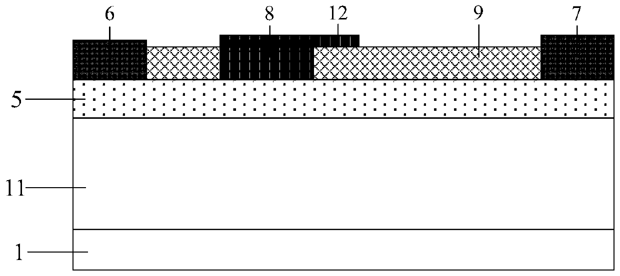
[0030] Figure 4 A RESURF HEMT device with an N-type floating buried layer is shown. This example device includes:

[0031] Substrate 1, buffer layer 2 located on top of substrate 1, N-type channel layer 4 located on top of buffer layer 2, barrier layer 5 located on top of channel layer 4, and passivation layer 9 located on top of barrier layer 5 ; Both ends of the upper surface of the barrier layer 5 are respectively provided with a source electrode 6 and a drain electrode 7, and a gate electrode 8 is provided between the source electrode 6 and the drain electrode 7; the source electrode 6 and the drain electrode 7 are ohmic contact . It is characterized in that the buffer layer 2 is P-type doped, the P-type buffer layer 2 has an N-type floating buried layer 3, and the N-type floating buried layer 3 is spaced from the channel layer 4; the The N-type floating buried layer 3 horizontally extends from below the drain electrode 7 to between the gate electrode 8 and the drain e...

Embodiment 2

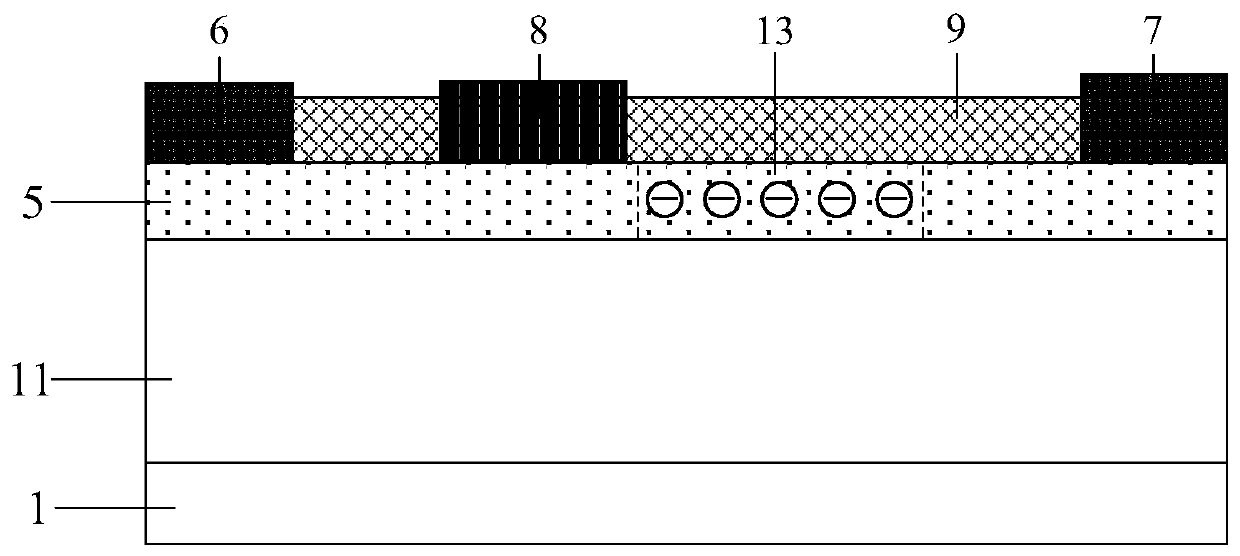
[0034] Compared with Example 1, the N-type floating buried layer of the device in this example is a multi-layer structure, and other structures are the same as those in Example 1, such as Figure 5 shown. Since the multi-layer N-type floating buried layer and the P-type buffer layer form multiple PN junctions, the vertical depletion width of the device can be further expanded, so as to further improve the electric field concentration effect at the drain electrode terminal and optimize the surface electric field of the device to increase the breakdown voltage.

Embodiment 3

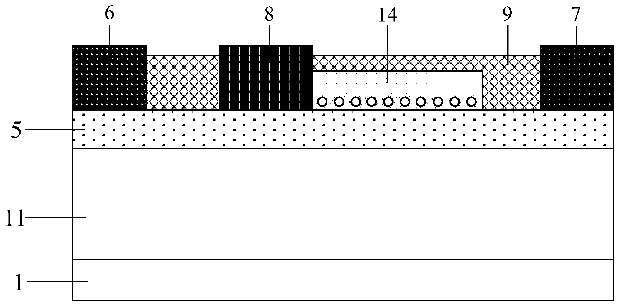
[0036] Compared with Embodiment 1, the N-type floating buried layer of the device in this example is doped laterally, and the other structures are the same as those of Embodiment 1, such as Image 6 shown. Compared with Example 1, the use of lateral segmented doping can further optimize the electric field distribution in the body, increase the average electric field strength, and further improve the off-state breakdown voltage of the device.


PUM


Abstract

The invention belongs to the technical field of a semiconductor, and relates to an RESURF HEMT device with an N type floating buried layer. According to a technical scheme, a P type buffer layer and the N type floating buried layer are introduced; a RESURF effect is formed by 2DEG at the P type buffer layer and a channel so as to modulate a transverse electric field of a device; a PN junction is formed by the N type floating buried layer and the P type buffer layer; in a blocking state, internal electric field distribution in the N type floating buried layer is modulated, and an electric field concentration effect at an drain electrode end is effectively improved, without introducing an additional parasitic capacitor; and meanwhile, a new electric field peak is introduced at the left side tail end of the N type floating buried layer, so that the electric field distribution on the surface of the device can be more uniform, and the breakdown voltage of the device is improved consequently. The preparation process of the device disclosed by the invention is compatible with a conventional process.

Description

technical field [0001] The invention belongs to the technical field of semiconductors, and specifically relates to a high electron mobility transistor (High Electron Mobility Transistor, HEMT) device. Background technique [0002] High electron mobility transistors (HEMTs) based on GaN materials, due to high electron saturation velocity, high density two-dimensional electron gas (2DEG), and high critical breakdown electric field, make them suitable for high current, low power consumption, high frequency and high voltage. Switch applications have huge application prospects. [0003] The key to power switching devices is to achieve high breakdown voltage, low on-resistance and high reliability. The critical breakdown electric field of GaN material is ten times that of Si. At present, the withstand voltage of GaN power devices is far from reaching its theoretical limit. The reason is that The gate electric field concentration effect causes the device to break down early, and t...

Claims


Application Information

Patent Timeline
Patent Type & Authority Patents(China)
IPC IPC(8): H01L29/778H01L29/06
CPCH01L29/063H01L29/778
Inventor 罗小蓉彭富杨超吴俊峰魏杰邓思宇张波李肇基
Owner UNIV OF ELECTRONICS SCI & TECH OF CHINA
Why Eureka
Try Eureka