Method of generating strong spin waves and spin devices for ultra-high speed information processing using spin waves

a technology of spin waves and information processing, applied in the direction of pulse techniques, instruments, magnetic bodies, etc., can solve the problems of increasing current density, shortening of conducting wires, and limited cmos-based information processing methods

Active Publication Date: 2012-04-24
SEOUL NAT UNIV R&DB FOUND
View PDF4 Cites 7 Cited by
  • Summary
  • Abstract
  • Description
  • Claims
  • Application Information

AI Technical Summary

Benefits of technology

[0087]Advantages and features of the present invention, and a method for achieving them will be clarified with reference to embodiments that will be described later. The invention may, however, be embodied in many different forms and should not be construed as being limited to the embodiments set forth herein; rather, these embodiments are provided so that this disclosure will be thorough and complete, and will fully convey the concept of the invention to those skilled in the art.

Problems solved by technology

CMOS-based information processing methods are expected to be limited for the following reasons.
However, when the thickness of the gate oxide layer is about 0.7 nm, electrons transmit the gate oxide layer and the gate oxide layer does not serve as an insulating layer any more.
Secondly, when the widths of conducting wires are reduced for improvements in the integration degree, a short of the conducting wires occurs due to an increase of current density.
However, since an induction field due to a current flowing through the conducting wire is formed to a size that is in inverse proportion to a distance even in a distant area from the conducting wire, in a device using an existing magnetostatic wave, all areas of the device are included in the effect of a magnetic field and spin waves cannot be generated in a local area.
However, a study for using exchange spin waves and dipole-exchange spin waves in a device has proceeded hardly.
However, a method of generating spin waves by the supply of the energy presented here is just a general method of generating spin waves in a magnetic material, and a method of generating strong spin waves in a local area for the use in an information processing device for spin waves has not been presented.

Method used


Image

  • Method of generating strong spin waves and spin devices for ultra-high speed information processing using spin waves
  • Method of generating strong spin waves and spin devices for ultra-high speed information processing using spin waves
  • Method of generating strong spin waves and spin devices for ultra-high speed information processing using spin waves

Examples


first embodiment

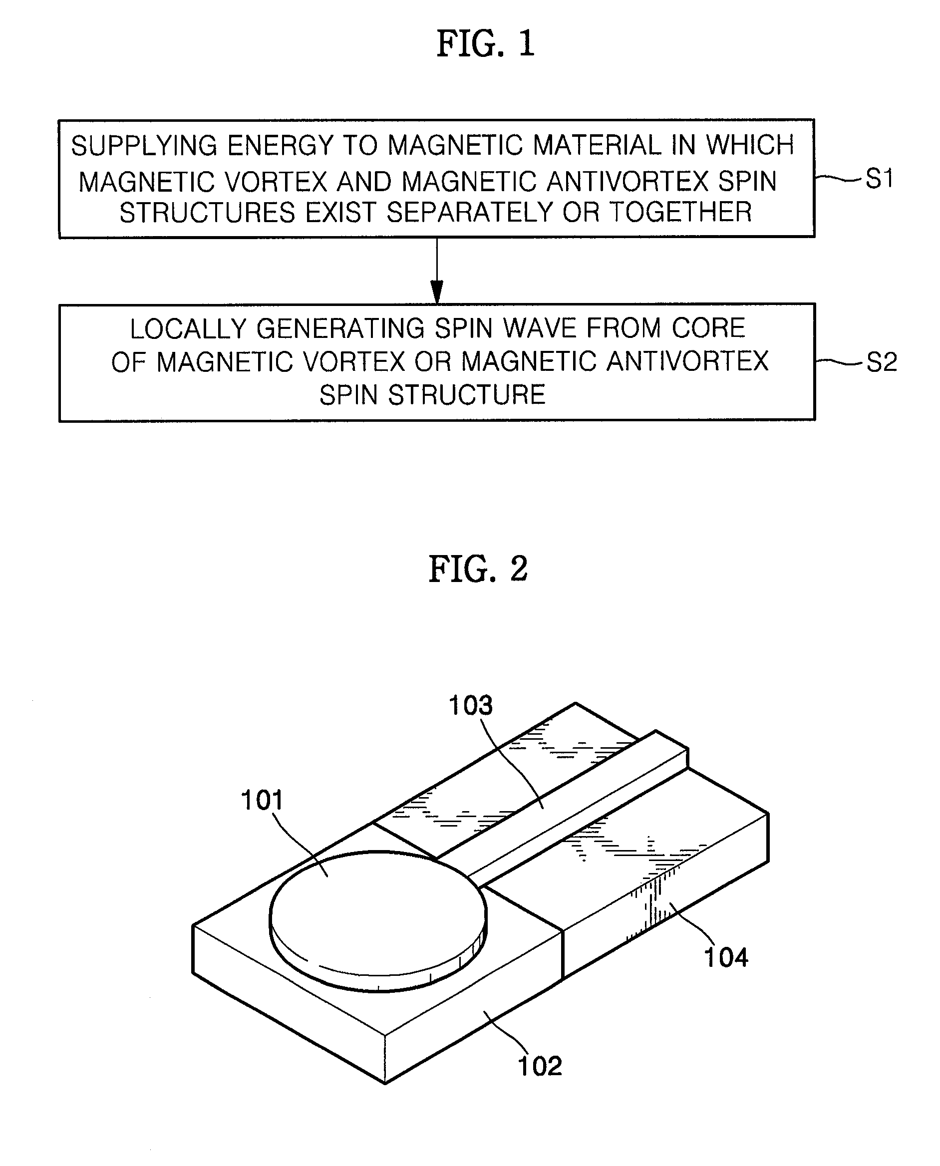
[0088]FIG. 1 is a flowchart illustrating a method of generating spin waves according to an embodiment of the present invention.

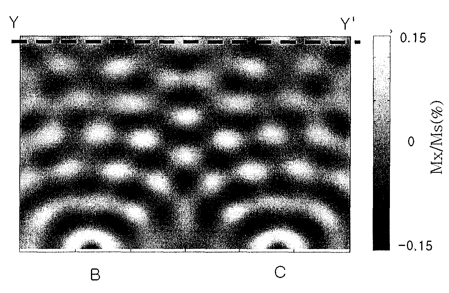
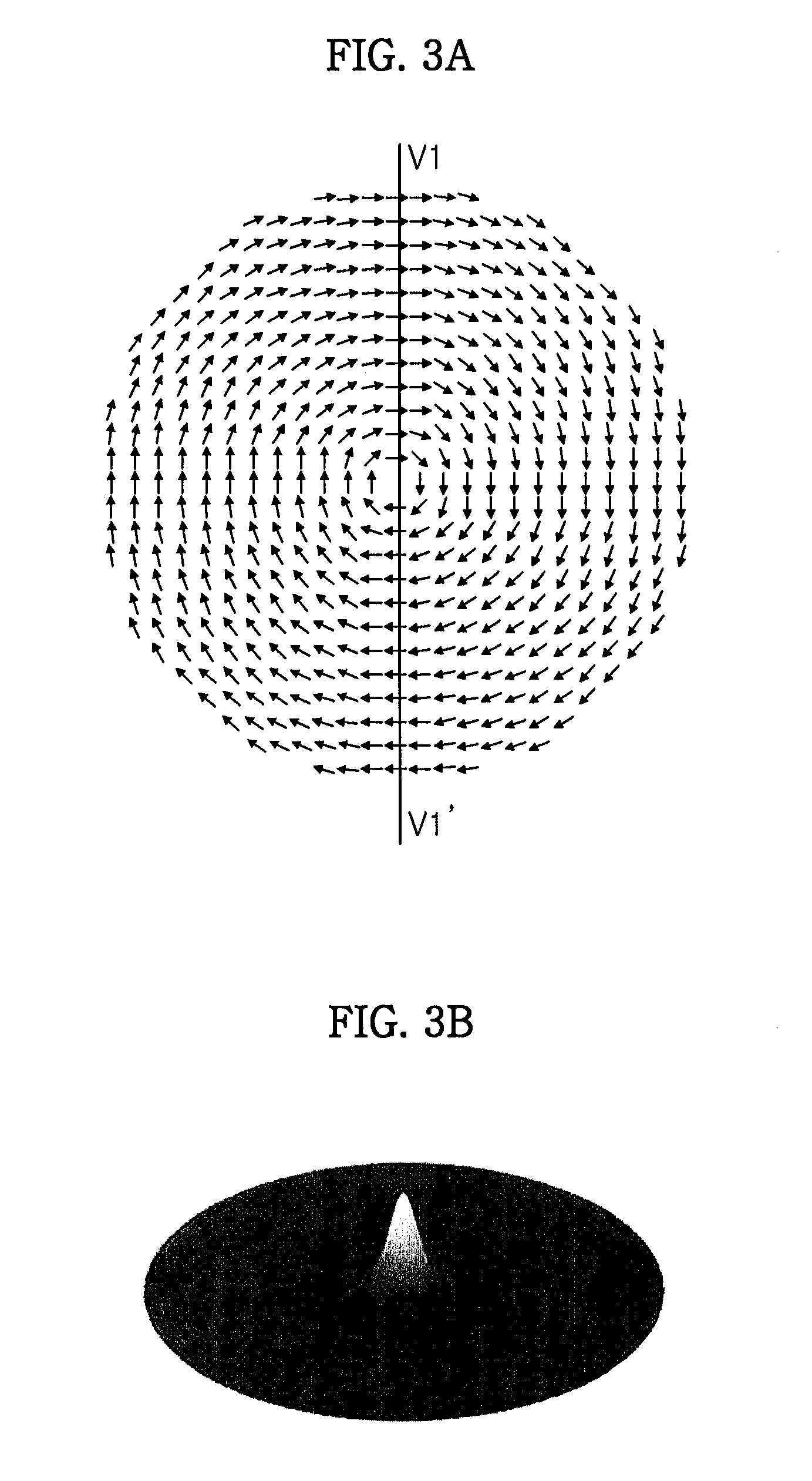
[0089]Referring to FIG. 1, in the method of generating spin waves according to the present invention, an energy is supplied to a magnetic material in which magnetic vortex and magnetic antivortex spin structures exist separately or together (operation S1). Owing to the supply of the energy, spin waves are locally generated from a core of a magnetic vortex or magnetic antivortex spin structure (operation S2). In this case, spin waves can be locally generated from a core of the magnetic vortex or magnetic antivortex spin structure or while two vortexes collide with each other and annihilate, and simultaneously, electromagnetic waves having the same frequencies as those of the generated spin waves can be generated . A specific principle of generating the magnetic vortex, the magnetic antivortex spin structures and spin waves will be described later.

[0090]Like i...

second embodiment

[0109]In the spin wave device illustrated in FIG. 2, the spin wave-generating unit 101 has a circular thin film shape. However, the shape of the spin wave-generating unit 101 in the spin wave device according to the present invention is not limited to this. Only, when the shape and dimension of the spin wave-generating unit 101 are decided, the above-described magnetic vortex and magnetic antivortex spin structures should exist separately or together in a stable state.

[0110]FIG. 9 illustrates possible shapes as the shape of a spin wave-generating unit in the spin wave device according to the present invention. As illustrated in FIG. 9, examples of shapes of the spin wave-generating unit may include a rectangular shape, a circular shape, a triangular shape, a rectangular shape having circular arc-shaped edges, a triangular shape having rounded edges, a quadrangular shape, a peanut shape, a dumbbell shape, and a rectangular shape having circular arc-shaped extended left and right side...

third embodiment

[0111]The energy-supplying unit 102 supplies an energy to the spin wave-generating unit 101. Here, one of a magnetic field, an electric field, a voltage, a current, an electromagnetic wave, sound, heat, and a magnetoelastic energy acts on the spin wave-generating unit 101 separately or compositely and causes the formation of a local torque. The energy-supplying unit 102 may have various shapes and materials according to kinds of applied energies.

[0112]FIG. 10A illustrates an embodiment of the case where the energy-supplying unit 102 supplies a magnetic field energy. Here, the spin wave-generating unit 101 and the spin-wave waveguide 103 are supported on the substrate 104. Specifically, the energy-supplying unit 102 includes a magnetic field-applying conducting wire 201 formed of metallic wires at both sides of the substrate 104 under the spin wave-generating unit 101, and a power supply unit 202. Here, a magnetic field is applied to a portion or the entire surface of the spin wave-g...


PUM

PropertyMeasurementUnit
thicknessaaaaaaaaaa
sizeaaaaaaaaaa
frequencyaaaaaaaaaa

Abstract

Provided are a method of generating strong spin waves, a method of simultaneously generating spin waves and electromagnetic waves, a logic operation device using spin waves, a variety of spin wave devices employing the same, and a method of controlling phases of spin waves. In the method of generating spin waves, strong spin waves are generated by supplying various shapes of energies to a magnetic material in which a magnetic vortex and magnetic antivortex spin structures exist separately or together. In the logic operation device, wave factors of frequency, wavelength, amplitude, and phase of a spin wave generated by the method of generating spin waves are controlled and wave characteristics such as reflection, refraction, transmission, tunneling, superposition, interference, and diffraction are used.

Description

TECHNICAL FIELD[0001]The present invention relates to a method and a device for generating strong spin waves, and more particularly, to a method of generating a dipole-exchange spin wave having a wavelength of several nm to several μm and having a frequency band of several hundreds of MHz to several tens of GHz and a device for generating spin waves having a configuration for implementing the method, and an information processing device to perform logic operations using the spin waves. In the present specification, a device for generating spin waves and an information processing device using the same are referred to as spin wave devices.BACKGROUND ART[0002]CMOS-based information processing methods are expected to be limited for the following reasons. Firstly, the thickness of a gate oxide layer should be gradually decreased as an integration degree is improved. However, when the thickness of the gate oxide layer is about 0.7 nm, electrons transmit the gate oxide layer and the gate o...

Claims


Application Information

Patent Timeline
Patent Type & Authority Patents(United States)
IPC IPC(8): G11B5/66H01L27/105
CPCG11C11/16G11C13/06H03K19/168H03B15/006H01F1/401H01F1/408G11C11/161G11C11/1675G11B5/66H01L27/14601
Inventor KIM, SANG-KOOGLEE, KI-SUKCHOI, SANG-KOOK
Owner SEOUL NAT UNIV R&DB FOUND
Why Eureka
Try Eureka