
Electrophotographic photoconductor, image forming apparatus using the same, and process cartridge

a photoconductor and photoconductor technology, applied in the field of electrographic photoconductor, image forming apparatus using the same, and process cartridges, can solve the problems of photosensitivity tending to degrade, image degradation due to image blur, and superior user-friendliness, so as to prevent the increase of residual potential and improve the effect of image degradation

Active Publication Date: 2012-05-08
RICOH KK
View PDF41 Cites 2 Cited by
  • Summary
  • Abstract
  • Description
  • Claims
  • Application Information

AI Technical Summary

Benefits of technology

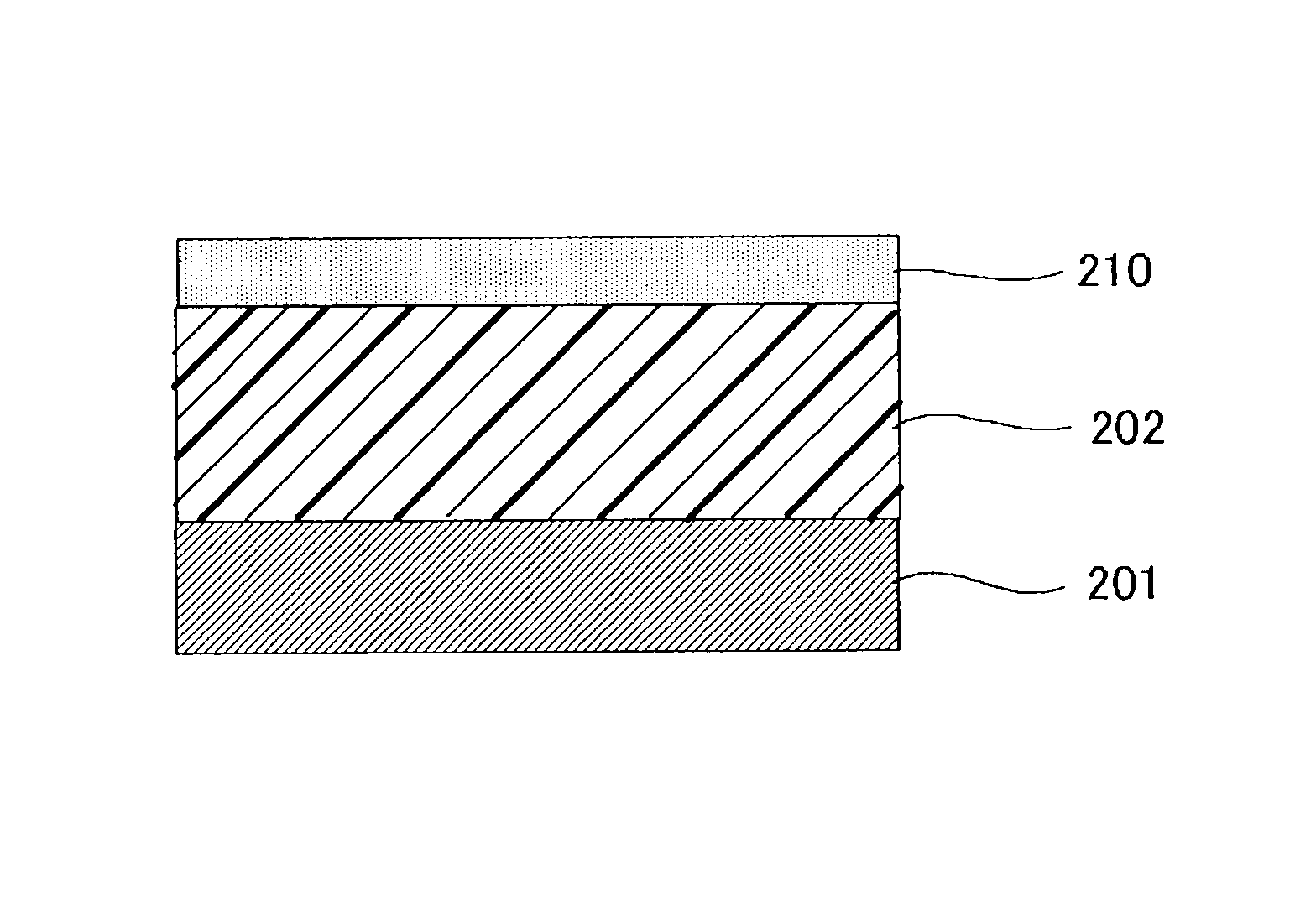
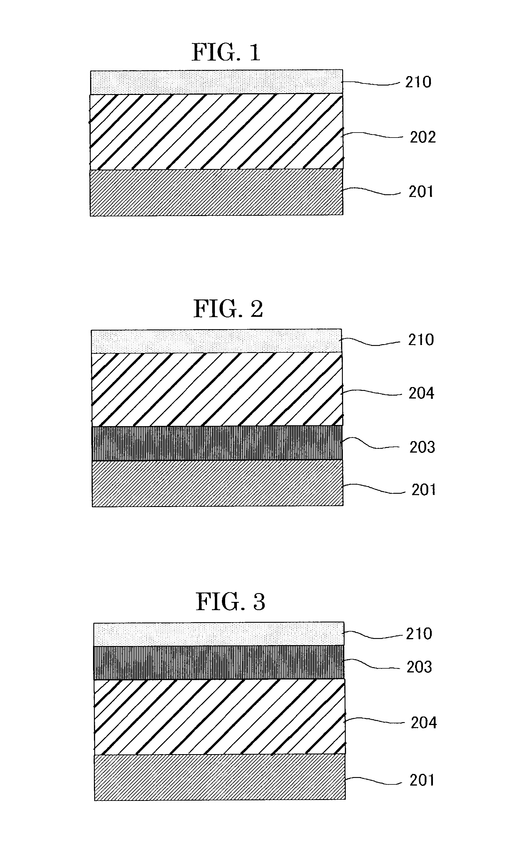
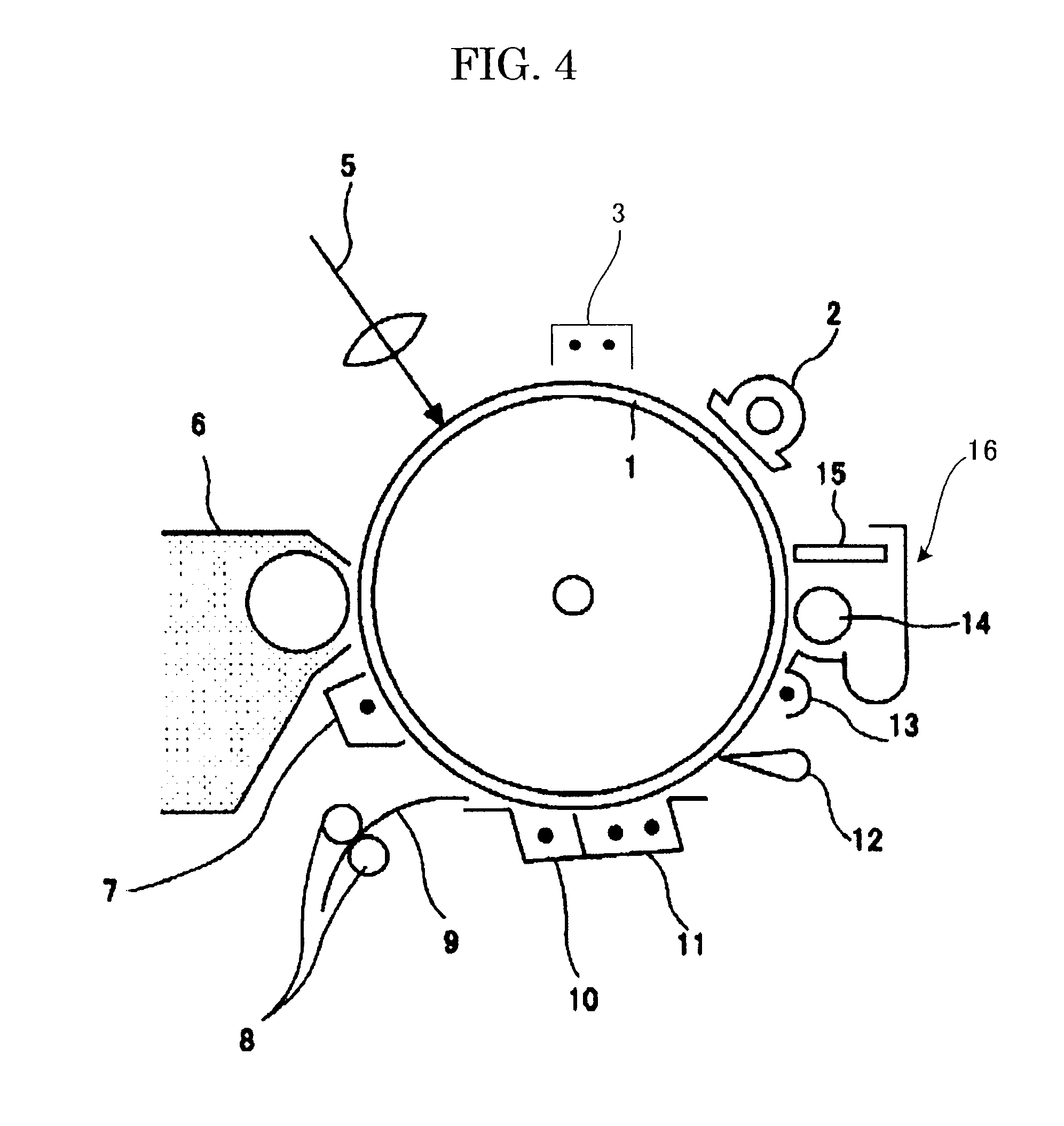
[0017]The present invention aims to provide an electrophotographic photoconductor containing a filler in its surface protective layer serving as the outermost surface layer, which is capable of realizing higher speed image formation by reducing the initial residual potential, reducing image degradation due to the occurrence of image blurring, and suppressing an increase in residual potential and the occurrence of interface cracking, thereby stably forming a high-quality image even when repeatedly used for a long period of time, and to provide an image forming apparatus using the electrophotographic photoconductor, and a process cartridge using the electrophotographic photoconductor.
[0018]The present inventors carried out extensive studies and examinations in order to reduce the initial residual potential and solve the problem with image degradation due to image blur and the problem with an increase in residual potential and have found the following results. Specifically, the present inventors have found that although it has been conventionally considered that when a charge transporting material having a low oxidation potential is contained in a photosensitive layer of a photoconductor, and a charge transporting material having an oxidation potential higher than that of the charge transporting material contained in the photosensitive layer is contained in a surface protective layer of the photoconductor, a difference in oxidation potential of the charge transporting materials contained in each of the photosensitive layer and the surface protective layer forms a barrier to charge injection, leading to a decrease in charge transporting rate and suppression of an increase in residual potential, when a surface protective layer is not so thick in a photoconductor having a layer configuration where a photosensitive layer and the surface protective layer are provided, it is possible to suppress the increase in residual potential and stably form a high-quality image at high-speed even though the photoconductor is repeatedly used.

Problems solved by technology

Photoconductors (OPCs) using organic photoconductive materials are widely used for laser printers and digital copiers using electrophotography, due to their cost, manufacturability, and non-polluting properties.
However, each photosensitive layer of the organic photoconductors (OPCs) is easily peeled off by repetitive use, and therefore the potential of the photoconductors tends to decrease and the photosensitivity tends to degrade.
Further, a scratch on a surface of the photoconductor tends to cause background smear, and degradation in image density and quality of the resultant images.
However, another problem occurs when these methods are used to prevent the abrasion of the photoconductor.
Specifically, oxidized gases, such as ozone and NOx arising due to use conditions or environment, adhere to the surface of the photosensitive layer and decrease the surface resistance thereof, resulting in a problem such as blurring of the resultant images.
Meanwhile, when a conductive filler is used in the surface protective layer, the outline of an image is blurred, i.e., so-called image blur is caused, resulting in a significant influence upon the image quality, although the electrical resistance is reduced and the influence on the increase in residual potential is relatively small.
It is known that when the method of incorporating a filler into the surface protective layer is employed in order to reduce abrasion of the photosensitive layer, ozone, NOx or other oxidative substances caused by the repetitive use of the photoconductor and the environment surrounding the photoconductor adsorb onto the surface protective layer, and the electrical resistance of the photoconductor decreases depending on the frequency of use and the use environment, causing a problem such as image flow (image blur), etc.
In order to decrease the influence of substances causing the blurred images, a method of adding an additive such as an antioxidant in the surface protective layer is effective, however, the additive typically does not have photoconductivity, and therefore the addition of much amount thereof in the surface protective layer causes problems such as degradation of sensitivity and increase of residual potential of the resultant photoconductor.
For this reason, there is a trade-off relation therebetween, which makes it difficult to solve the problem.
The increase in residual potential which is often observed when a filler having high insulating property is used in a surface protective layer of a photoconductor leads to a high-electric potential at bright areas in the image forming apparatus, causing degradation of image density and gray-scale properties.
However, when the electric potential is increased at dark areas in an image forming apparatus, the intensity of the electric field is increased, leading to not only an image defect, such as background smear, but also the shortening of the longevity of the photoconductor.
For this reason, it is hard to use a filler having high insulation property.
Although the occurrence of image blurring can be reduced by heating the photoconductor, this poses a great obstacle to the downsizing of an image forming apparatus, reduction of power consumption, and shortening of the start-up time of an image forming apparatus.
However, the charging unit utilizing corona discharge cause a generation amount of discharge products (ozone, NOx, etc.) greater than the roller charging units cause.
When a photoconductor containing a filler in the outermost surface layer is used in an attempt to achieve high durability, image blur is liable to occur.

Method used


Image

  • Electrophotographic photoconductor, image forming apparatus using the same, and process cartridge
  • Electrophotographic photoconductor, image forming apparatus using the same, and process cartridge
  • Electrophotographic photoconductor, image forming apparatus using the same, and process cartridge

Examples


synthesis example 1

Synthesis of Titanylphthalocyanine Crystal

[0475]The synthesis of titanylphthalocyanine crystal was carried out in accordance with the method described in Japanese Patent Application Laid-Open (JP-A) No. 2004-83859. Specifically, 292 g of 1,3-diminoisoindoline, and 1,800 g of sulfolane were mixed, and 20.4 g of titanium tetrabuthoxide was delivered by drops into the mixture under nitrogen gas stream. After completion of the dropping, the mixture was gradually raised in temperature to 180° C. and stirred for 5 hours while maintaining the reaction temperature from 170° C. to 180° C. so that the components were reacted. After completion of the reaction, the reaction product was left standing to cool, and then the precipitate was filtered and washed with chloroform until the powder turned blue. Next, the powder washed with methanol several times, further washed with 80° C. hot water several times, and the dried, thereby obtaining a coarse titanylphthalocyanine.

[0476]The coarse titanylpht...

example 1

Production of Electrophotographic Photoconductor

[0524]An electrophotographic photoconductor of Example 1 was produced in a similar manner to that described in Comparative Example 7, except that is the charge transporting material for the surface protective layer was changed to a charge transporting material having the following structural formula (oxidation potential: 0.89V vs SCE, melting point: 93.5° C.).

[0525]

example 2

Production of Electrophotographic Photoconductor

[0526]An electrophotographic photoconductor of Example 2 was produced in a similar manner to that described in Comparative Example 8, except that the charge transporting material for the surface protective layer was changed to a charge transporting material having the following structural formula (oxidation potential: 0.89V vs SCE, melting point: 93.5° C.).

[0527]


PUM


Abstract

The present invention provides an electrophotographic photoconductor which includes at least a photosensitive layer and a surface protective layer over a support, wherein the surface protective layer contains a filler, a charge transporting material and a specific compound; and the photosensitive layer contains at least a charge transporting material; the charge transporting material contained in the photosensitive layer has an oxidation potential lower than the oxidation potential of the charge transporting material contained in the surface protective layer and is a specific compound.

Description

BACKGROUND OF THE INVENTION[0001]1. Field of the Invention[0002]The present invention relates to an electrophotographic photoconductor used in image formation based on electrophotography, for example, in copiers, electrostatic printing, printers, facsimiles, and electrostatic recording. The present invention also relates to an image forming apparatus using the electrophotographic photoconductor and a process cartridge using the electrophotographic photoconductor.[0003]2. Description of the Related Art[0004]Information processing systems using electrophotography are making remarkable progress recently. Particularly, laser printers and digital multifunction processing machines, in which information is converted into digital signals and recorded by means of light, have been extremely improved in terms of printing quality and reliability. Further, technologies used in these laser printers and digital copiers are applied to laser printers and digital copiers capable of printing full-colo...

Claims


Application Information

Patent Timeline
Patent Type & Authority Patents(United States)
IPC IPC(8): G03G15/06
CPCG03G5/0517G03G5/0521G03G5/0614G03G5/0666G03G5/0672G03G5/14708G03G5/061473
Inventor NAKAMORI, HIDEO
Owner RICOH KK
Learn More