High frequency helical amplifier and oscillator

a high-frequency helical amplifier and oscillator technology, applied in the field of amplification, millimeter and sub-millimeter wavelength generation, electron devices, etc., can solve the problems of fundamental issues such as thermal management and electron beam transmission and the inability to meet the helix in tim

Active Publication Date: 2012-05-15
TERAPHYSICS CORP
View PDF16 Cites 12 Cited by
  • Summary
  • Abstract
  • Description
  • Claims
  • Application Information

AI Technical Summary

Benefits of technology

[0010]Further scope of the applicability of the present invention will become apparent from the detailed description provided below. It should be understood, however, that the detailed description and specific examples, while indicating preferred embodiments of the invention, are given by way of illustration only, since various changes and modifications within the spirit and scope of the invention will become apparent to those skilled in the art.

Problems solved by technology

Helical slow wave circuits are still used as high power millimeter wave traveling wave tube (TWT) amplifiers, producing as much as 200 Watts CW at 45 GHz, but fundamental issues associated with conventional fabrication, thermal management and electron beam transmission are obstacles to higher frequency applications.
Heat generated on the helix whether by electron beam interception or ohmic losses from the RF current must be conducted away through dielectric support rods that are inferior thermal conductors and which frequently make somewhat uncertain thermal contact with the helix.

Method used


Image

  • High frequency helical amplifier and oscillator
  • High frequency helical amplifier and oscillator
  • High frequency helical amplifier and oscillator

Examples


Embodiment Construction

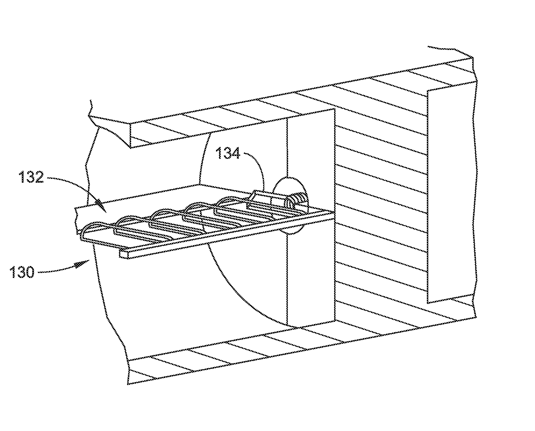
[0032]Disclosed herein is a miniature helical slow wave structure in which the helix is fabricated by selectively plating metal into a lithographically patterned circular trench fabricated by reactive ion etching of a silicon wafer. The helix is supported by diamond dielectric support rods. Diamond is the best possible thermal conductor, and it can be bonded to the helix. The electron beam is transmitted, not through the center of the helix, but around the outside. While all of this would be impractical at, say, C-Band, it is feasible to fabricate such a structure for operation in the mm and sub mm wavelength ranges. We shall describe this concept as it applies to both TWTs and BWOs.

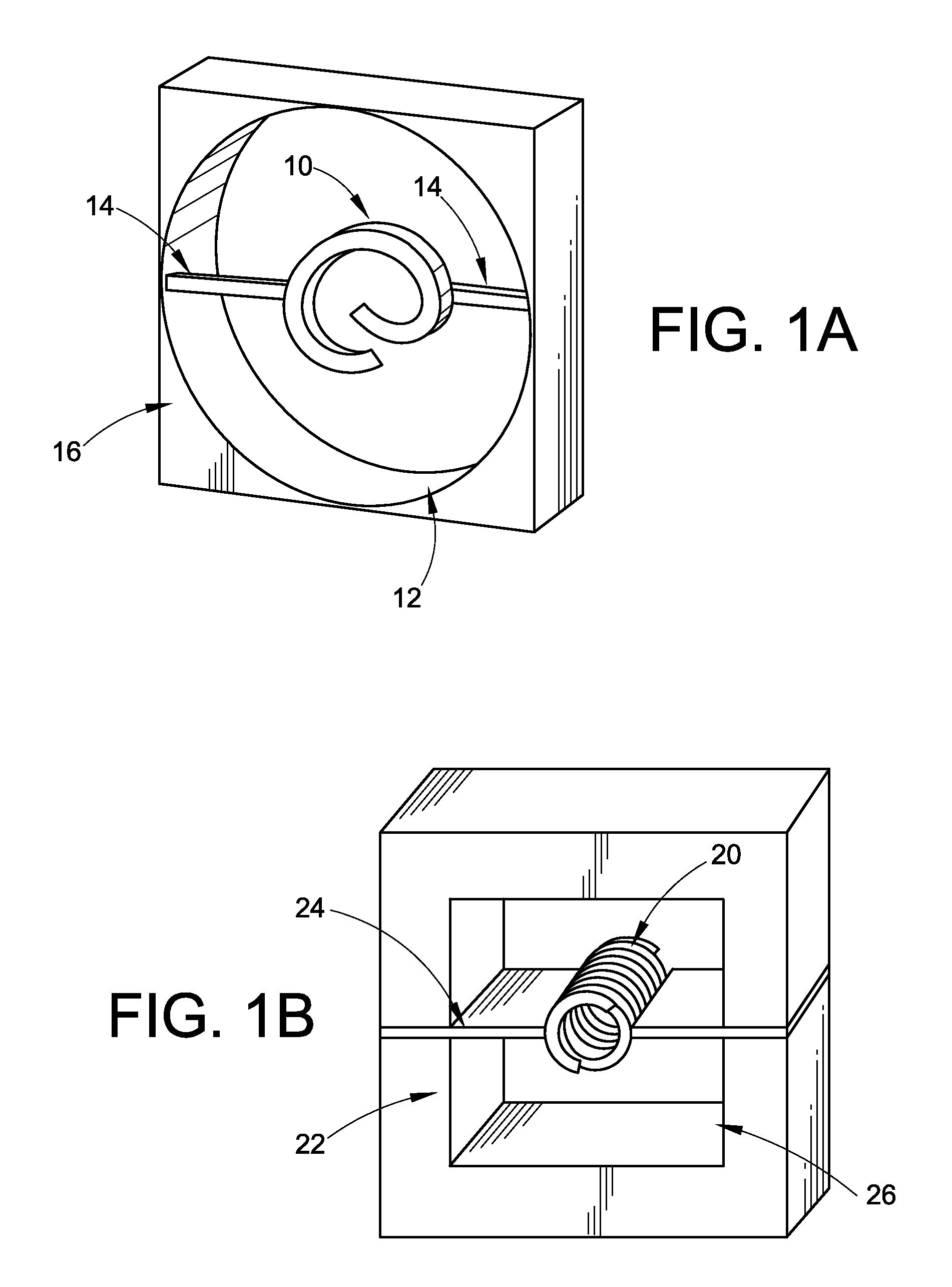
[0033]Referring now to the drawings wherein the showings are for purposes of illustrating the exemplary embodiments only and not for purposes of limiting the claimed subject matter, FIGS. 1A and 1B provide views of a miniature helical slow wave circuit. As shown in FIG. 1A, a single turn of helix 10 may ...


PUM


Abstract

Disclosed herein is a class of mm and sub mm wavelength amplifiers and oscillators operating with miniature helical slow wave circuits manufactured using micro fabrication technology. The helices are supported by diamond dielectric support rods. Diamond is the best possible thermal conductor, and it can be bonded to the helix. The electron beam is transmitted, not through the center of the helix, but around the outside. In some configurations the RF power produced may be radiated directly from the slow wave circuit. The method of fabrication, which is applicable above 60 GHz, is compatible with mass production.

Description

PRIORITY[0001]This application claims the benefit of U.S. Provisional Application No. 60 / 902,537, filed Feb. 21, 2007.STATEMENT REGARDING FEDERALLY SPONSORED RESEARCH[0002]Financial assistance for this project was provided in accordance with U.S. Government Contract Nos. FA9550-07-C-0076, FA9550-06-C-0081, W911NF-06-C-0086, and W911NF-06-C-0026, and the United States Government may own certain rights to this invention.BACKGROUND OF THE INVENTION[0003]The present invention relates to the millimeter and sub millimeter wavelength generation, amplification, and processing arts. It particularly relates to electron devices such as traveling wave tubes for millimeter and sub mm wavelength amplifiers and oscillators, and will be described with particular reference thereto. However, the invention will also find application in other devices that operate at millimeter and sub mm wavelengths, and in other devices that employ slow wave circuits.[0004]A traveling wave tube (TWT) is an electron de...

Claims


Application Information

Patent Timeline
Patent Type & Authority Patents(United States)
IPC IPC(8): H01J25/34
CPCH01J25/34H01J23/26
Inventor DAYTON, JR., JAMES A.KORY, CAROL L.
Owner TERAPHYSICS CORP
Why Eureka
Try Eureka