Semiconductor memory device with stacked memory cell and method of manufacturing the stacked memory cell

a memory cell and semiconductor technology, applied in semiconductor devices, digital storage, instruments, etc., can solve problems such as the increase of the integration density of the pram

Active Publication Date: 2012-05-15
SAMSUNG ELECTRONICS CO LTD
View PDF41 Cites 121 Cited by
  • Summary
  • Abstract
  • Description
  • Claims
  • Application Information

AI Technical Summary

Benefits of technology

[0014]The present invention provides a phase-change memory cell with improved integration density.
[0032]Embodiments of the present invention also provide a resistive-change memory cell with improved integration density.

Problems solved by technology

However, there is a restriction to reducing a size of a control transistor of a conventional memory cell, which supplies current required to generate the Joule heat, thereby preventing an increase in the integration density of the PRAM.

Method used


Image

  • Semiconductor memory device with stacked memory cell and method of manufacturing the stacked memory cell
  • Semiconductor memory device with stacked memory cell and method of manufacturing the stacked memory cell
  • Semiconductor memory device with stacked memory cell and method of manufacturing the stacked memory cell

Examples


Embodiment Construction

[0085]Hereinafter, exemplary embodiments of the present invention will be described in detail with reference to the accompanying drawings. Like reference numerals are used to designate like or equivalent elements throughout this disclosure.

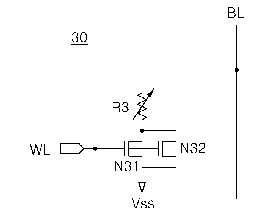
[0086]A cell structure of a semiconductor memory device according to an embodiment of the present invention will now be described with reference to FIGS. 3 and 4. In this embodiment, the semiconductor memory device indicates a phase-change random access memory (PRAM) formed of a phase-change material.

[0087]Referring to FIG. 3A, a phase-change memory cell 30 includes first and second control transistors N31 and N32 on different layers, and a variable resistance device R3 formed of a phase-change material.

[0088]Gates of the first and second control transistors N31 and N32 are connected to a word line WL. A first terminal of each of the first and second control transistors N31 and N32 is connected to a reference voltage, e.g., a ground voltage Vss.

[0...


PUM


Abstract

In a semiconductor memory device and method, resistive-change memory cells are provided, each including a plurality of control transistors formed on different layers and variable resistance devices comprising a resistive-change memory. Each resistive-change memory cell includes a plurality of control transistors formed on different layers, and a variable resistance device formed of a resistive-change memory. In one example, the number of the control transistors is two. The semiconductor memory device includes a global bit line; a plurality of local bit lines connected to or disconnected from the global bit line via local bit line selection circuits which correspond to the local bit lines, respectively; and a plurality of resistive-change memory cell groups storing data while being connected to the local bit lines, respectively. Each of the resistive-change memory cells of each of the resistive-change memory cell groups comprises a plurality of control transistors formed on different layers, and a variable resistance device formed of a resistive-change memory. In addition, the semiconductor memory device has a hierarchical bit line structure that uses a global bit line and local bit lines. Accordingly, it is possible to increase both the integration density of the semiconductor memory device and the amount of current flowing through each of the resistive-change memory cells.

Description

RELATED APPLICATIONS[0001]This application is a continuation-in-part application of U.S. Ser. No. 11 / 238,381, filed Sep. 29, 2005, which claims the priority of Korean Patent Application Nos. 10-2004-0085804, filed on Oct. 26, 2004 and 10-2005-0034552, filed on Apr. 26, 2005 in the Korean Intellectual Property Office. The disclosures of all the above applications are incorporated herein by reference in their entirety.BACKGROUND OF THE INVENTION[0002]1. Field of the Invention[0003]The present invention relates to a semiconductor memory device, and more particularly, to a semiconductor memory device with a stacked memory cell.[0004]2. Description of the Related Art[0005]A Phase-change random Access Memory (PRAM) is formed of a phase-change material such as a chalcogenide alloy that changes into a first of two phases when it is heated and cooled, and changes into a second phase when it is heated and cooled again. Here, the two phases are crystalline and amorphous phases. The PRAM is dis...

Claims


Application Information

Patent Timeline
Patent Type & Authority Patents(United States)
IPC IPC(8): G11C11/00
CPCG11C5/02G11C7/18G11C11/15G11C11/56G11C11/5678G11C13/0004G11C13/0023G11C13/0026G11C13/003G11C13/0064G11C13/0069H01L27/24G11C2013/0071G11C2213/71G11C2213/74G11C2213/79H10B63/30H10B61/22H10B63/00
Inventor KIM, SUNG-MINYUN, EUN-JUNGSEO, JONG-SOOKIM, DU-EUNGCHO, BEAK-HYUNGKIM, BYUNG-SEO
Owner SAMSUNG ELECTRONICS CO LTD
Why Eureka
Try Eureka