Circuit board having electrically connecting structure and fabrication method thereof

a technology of circuit boards and electrical connections, applied in the field of circuit boards, can solve the problems of not using all electrode pads of semiconductor chips or passive components for electrical connection, cracking of chips, and ineffective spatial arrangement, so as to enhance the uniform distribution of electrical connection points, reduce the number of circuits in the circuit board, and prevent uneven stress distribution. the effect of uneven distribution

Active Publication Date: 2012-05-29
UNIMICRON TECH CORP
View PDF7 Cites 2 Cited by
  • Summary
  • Abstract
  • Description
  • Claims
  • Application Information

AI Technical Summary

Benefits of technology

[0010]In view of the aforesaid drawbacks of the prior art, an objective of the present invention is to provide a circuit board having an electrically connecting structure and a method for fabricating the same, so as to increase the quantity and density of circuits disposed in the circuit board without increasing the area of the circuit board.
[0011]Another objective of the present invention is to provide a circuit board having an electrically connecting structure and a method for fabricating the same, so as to avoid uneven distribution of stress in forming electrical connection between the circuit board and other electronic components.
[0016]Therefore, according to the circuit board having an electrically connecting structure and the method for fabricating the same in the present invention, the standalone metal pads are provided on the insulating protective layer, and the circuits are disposed in a portion of the insulating protective layer beneath the standalone metal pads, while the electrically connecting pads are absent from the portion of the insulating protective layer beneath the standalone metal pads. As a result, the quantity and density of circuits disposed in the circuit board can be increased, without having to increase the area of the circuit board. And, the standalone metal pads enhance uniform distribution of electrical connection points on the circuit board, thereby preventing uneven distribution of stress in forming electrical connection between the circuit board and other electronic components.

Problems solved by technology

However, not all electrode pads of the semiconductor chip or passive component are used for electrical connection.
This is important because uneven stress would cause delamination between the chip and the circuit board after an encapsulation process is completed, and excessive stress may even lead to cracking of the chip.
This arrangement is not spatially effective because the electrically connecting pads 102′ (not for electrical connection) occupy a certain space of the circuit board where functional circuits cannot be disposed, thereby unfavorable for high circuit-density circuit boards with circuits being formed more and more densely.

Method used


Image

  • Circuit board having electrically connecting structure and fabrication method thereof
  • Circuit board having electrically connecting structure and fabrication method thereof
  • Circuit board having electrically connecting structure and fabrication method thereof

Examples


Embodiment Construction

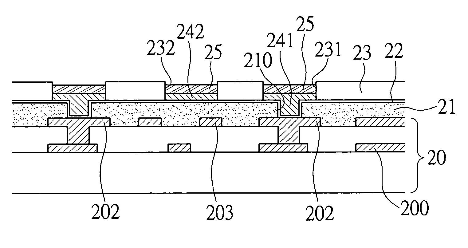
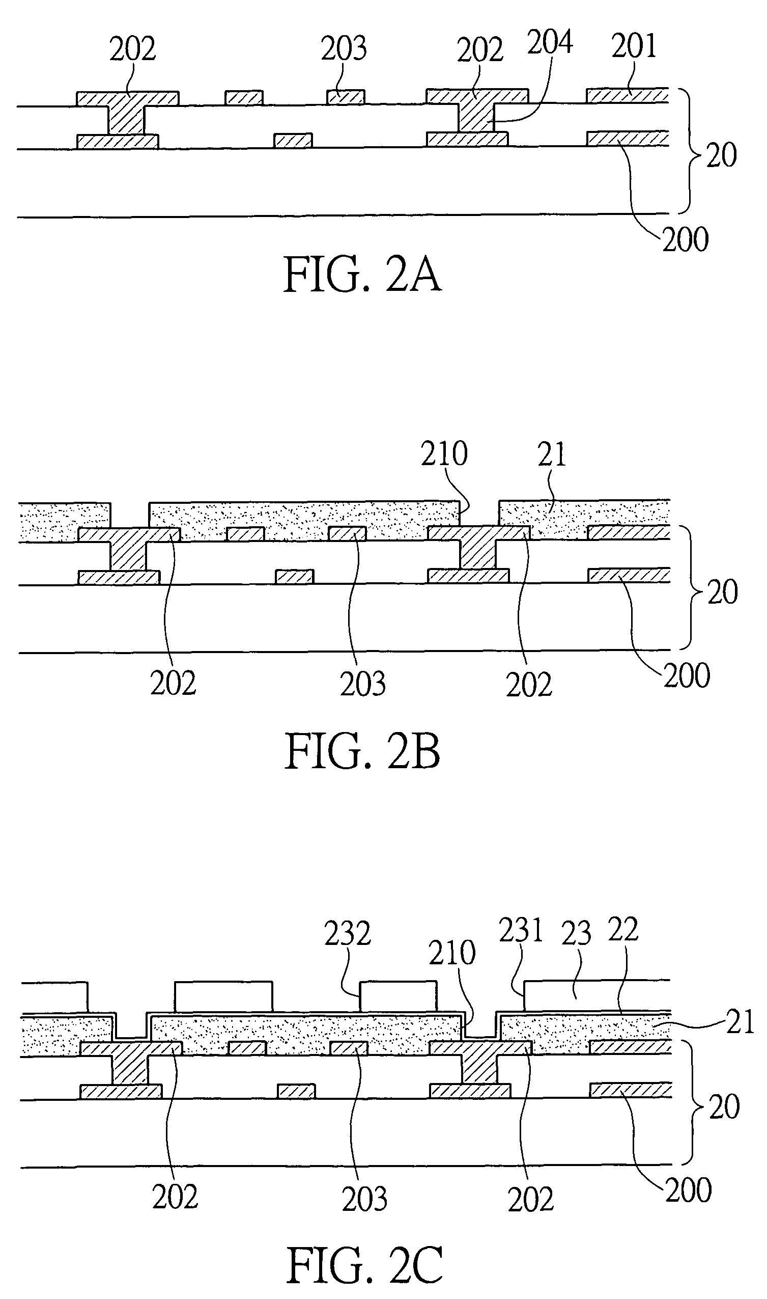
[0019]Preferred embodiments of a circuit board having an electrically connecting structure and a method for fabricating the same proposed by the present invention are described in detail as follows with reference to FIGS. 2A to 2F. It should be understood that the drawings are simplified schematic diagrams only showing the components relevant to the present invention, and the layout of components could be more complicated in practical implementation.

[0020]FIGS. 2A to 2F are cross-sectional views showing the steps of a method for fabricating a circuit board having an electrically connecting structure according to the present invention.

[0021]Referring to FIG. 2A, a circuit board body 20 having inner-layer circuits 200 is provided. A circuit layer 201 is formed on at least an outermost surface of the circuit board body 20. The circuit layer 201 comprises a plurality of electrically connecting pads 202 and circuits 203. A portion of the circuits 203 (not shown) is electrically connected...


PUM

PropertyMeasurementUnit
widthaaaaaaaaaa
widthaaaaaaaaaa
electricallyaaaaaaaaaa

Abstract

A circuit board having an electrically connecting structure and a method for fabricating the same are provided. A circuit board body having inner-layer circuits is provided. A circuit layer is formed on at least an outermost surface of circuit board body, and including electrically connecting pads and circuits. The electrically connecting pads are partially electrically connected to the circuits, and are partially electrically connected to the inner-layer circuits via conductive vias. An insulating protective layer is disposed on the circuit board body and is formed with openings therein for exposing the electrically connecting pads. Conductive posts are formed on the electrically connecting pads. Standalone metal pads are formed on the insulating protective layer but are not used for electrical connection. The conductive posts and electrically connecting pads are absent from the insulating protective layer beneath the standalone metal pads, such that circuits can be formed under the insulating protective layer.

Description

BACKGROUND OF THE INVENTION[0001]1. Field of the Invention[0002]The present invention relates to circuit boards and methods for fabricating the same, and more particularly, to a circuit board having an electrically connecting structure and a method for fabricating the circuit board.[0003]2. Description of the Prior Art[0004]The electronic industry has boomed and brought multi-functional and high-performance electronic products. For use with highly integrated and miniaturized semiconductor packages to incorporate more active components and package components therein, circuit boards having high-density circuit layout have been developed. The high-density circuit layout makes the circuit boards feasible for the miniaturized and multi-functional electronic products, allowing the circuit layout area in the circuit boards (having a limited space) to be increased by an interlayer connection technique, that is, more circuits and electronic components can be incorporated per unit area of the...

Claims


Application Information

Patent Timeline
Patent Type & Authority Patents(United States)
IPC IPC(8): H02B1/30
CPCH05K1/111H05K1/113H05K3/108H05K3/243Y10T29/49147H05K2201/0367H05K2201/09436H05K2201/09781H05K3/4007Y02P70/50
Inventor HU, WEN-HUNGCHI, WEN-YUAN
Owner UNIMICRON TECH CORP
Why Eureka
Try Eureka