Organic semiconductor radiation/light sensor and radiation/light detector

a radiation/light sensor and organic semiconductor technology, applied in the direction of instruments, semiconductor/solid-state device details, optical radiation measurement, etc., can solve the problems of poor sensitivity of organic semiconductors, and achieve the effects of improving dramatically detection efficiency, low energy loss capability, and high sensitivity

Active Publication Date: 2012-07-03
NIIGATA UNIVERSITY +1
View PDF14 Cites 2 Cited by
  • Summary
  • Abstract
  • Description
  • Claims
  • Application Information

AI Technical Summary

Benefits of technology

[0029]According to the organic semiconductor radiation / light sensor of the present invention, the carriers created by passage of radiation or light are avalanche-amplified by the high electric field generated near the signal amplification wire by means of applying the high voltage to the signal amplification wire, thus improving dramatically detection efficiency. Hence, even radiation such as rays exhibiting low energy loss capability or the like can be detected in real time with high sensitivity. Besides, the organic semiconductor is low in cost and is easy to deal with and further is flexible and therefore a radiation sensor applicable to new applications can be provided.
[0030]Further, the metal wire is used as the signal amplification wire. Hence, the organic semiconductor radiation / light sensor can be provided at low cost.
[0031]Furthermore, the signal amplification wire is 10 to 100 m in diameter. Hence, the carriers created by the passage of radiation or light can be certainly avalanche-amplified and besides the organic semiconductor radiation / light sensor can be made easy to deal with in its fabrication and in its use.
[0032]Moreover, the organic semiconductor is any one of polyaniline, polythiophene and polypyrrole. Hence, the organic semiconductor sensor can be provided at low cost.
[0033]Besides, the organic semiconductor is substantially columnar and then the signal amplification wire is arranged substantially parallel with a bottom of the organic semiconductor and further the electrode formed by deposition is provided on the upper surface of the organic semiconductor. Hence, the organic semiconductor radiation / light sensor can be provided which can be easily fabricated.
[0034]Further, the organic semiconductor is substantially columnar and the signal amplification wire is arranged on a central axis of the organic semiconductor and further the electrode formed by deposition is provided across an entire circumference of a lateral face of the organic semiconductor. Hence, an electric field within the sensor can be made uniform, permitting the organic semiconductor sensor with high sensitivity to be provided.

Problems solved by technology

The organic semiconductor, however, is presently poor in sensitivity as compared to the inorganic semiconductor due to an impact of its impurities, nonuniformity of polymer molecular mass, etc. thus not yet having come to practical use as a sensor of real-time radiation detection in the existing circumstances.Patent document 1: Japanese unexamined patent application publication No.

Method used


Image

  • Organic semiconductor radiation/light sensor and radiation/light detector
  • Organic semiconductor radiation/light sensor and radiation/light detector
  • Organic semiconductor radiation/light sensor and radiation/light detector

Examples


embodiment 1

(Embodiment 1)

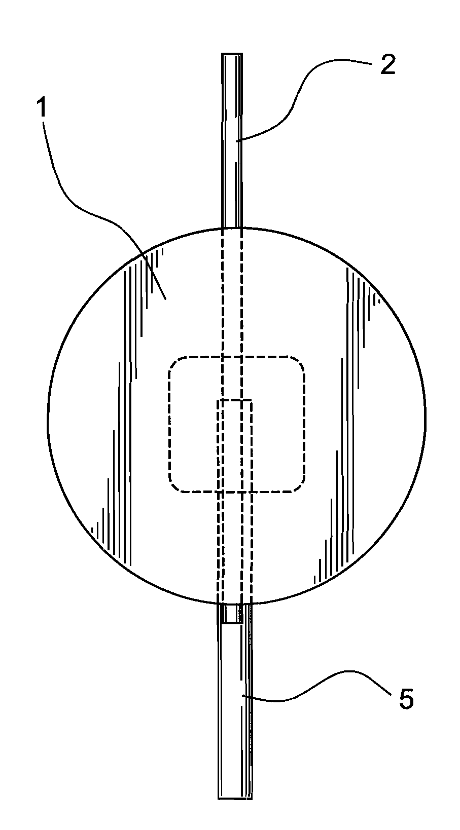
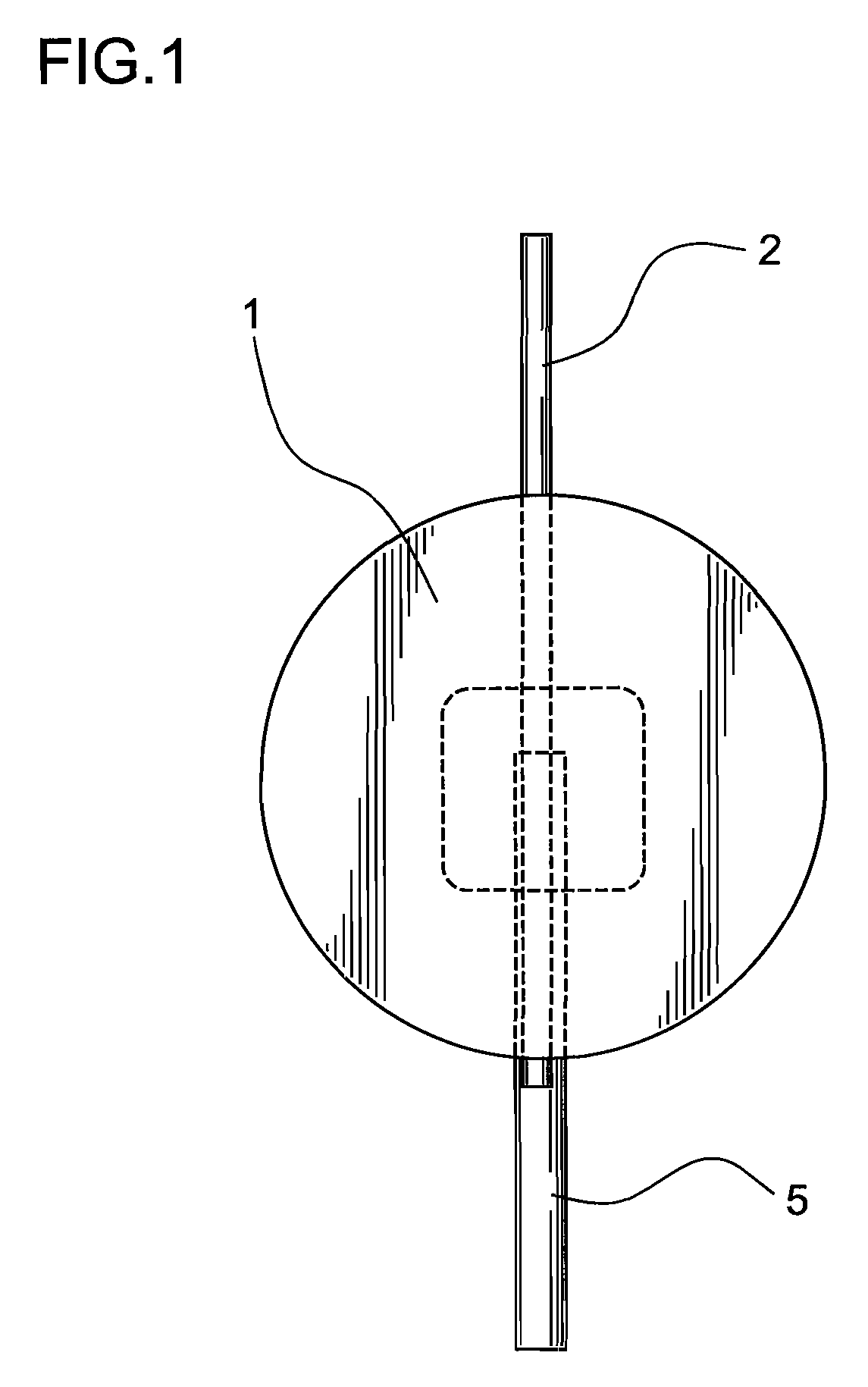
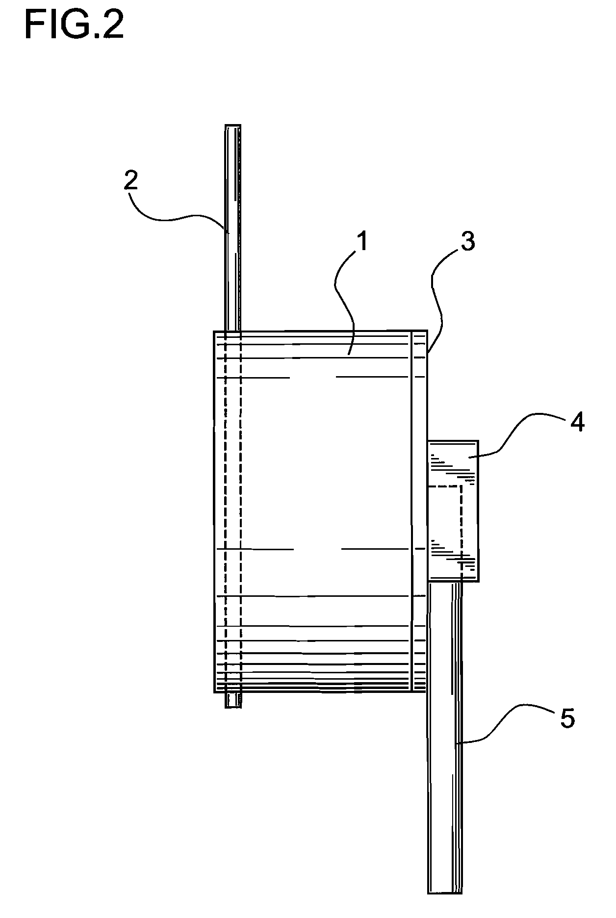
[0055]In FIG. 1 to FIG. 3, a first embodiment of the organic semiconductor radiation / light sensor and the radiation / light detector according to the present invention are shown.

[0056]Numeral symbol 1 denotes an organic semiconductor formed in a substantially columnar shape with 7 mm in diameter and 3 mm in thickness. In addition, the thicker the organic semiconductor 1, the larger, the number of carriers created by passage of radiation or light and thereby sensitivity of the organic semiconductor radiation / light sensor becomes higher.

[0057]Part of a signal amplification wire 2 is embedded in the organic semiconductor 1. This signal amplification wire 2 is arranged substantially parallel with one surface of the organic semiconductor 1 which is substantially columnar. In addition, in the present embodiment, for reasons of fabrication, the signal amplification wire 2 is embedded in a biased position near one surface of the organic semiconductor 1. To improve uniformity of ...

embodiment 2

(Embodiment 2)

[0077]In FIG. 6, shown is a second embodiment of an organic semiconductor radiation / light sensor according to the present invention.

[0078]Numeral symbol 11 denotes an organic semiconductor which is formed in a long and substantially columnar shape and is 10 mm in diameter and 50 mm in thickness. Part of a signal amplification wire 12 is embedded in the organic semiconductor 11. Then, the signal amplification wire 12 is arranged on a central axis of the organic semiconductor 11 which is substantially columnar. In the present embodiment, as in the first embodiment, polyaniline and a gold-plated tungsten wire with a circular cross section and 30 m in diameter are used for the organic semiconductor 11 and the signal amplification wire 12, respectively.

[0079]Besides, there is provided an electrode 13 which is formed by applying gold evaporation over an entire circumference in a lateral face of the organic semiconductor 11 formed in the substantially columnar shape. A lead w...

embodiment 3

(Embodiment 3)

[0084]Except that polyddecylthiophene (a test agent produced by Aldrich) has been used instead of polyaniline for the organic semiconductor 11 in the second embodiment, in a third embodiment, the organic semiconductor radiation / light sensor has been made in the same way as was done in the second embodiment. Also in this organic semiconductor radiation / light sensor, carriers created by passage of radiation or light are avalanche-amplified by a high electric field created near the signal amplification wire 12 by means of applying a high voltage to the signal amplification wire 12. Hence, as in the second embodiment, even radiation such as rays exhibiting smaller energy loss capability can be detected in real time with high sensitivity.


PUM

PropertyMeasurementUnit
diameteraaaaaaaaaa
diameteraaaaaaaaaa
diameteraaaaaaaaaa

Abstract

There is provided a high-sensitivity organic semiconductor radiation / light sensor and a radiation / light detector which can detect rays in real time. In the high-sensitivity organic semiconductor radiation / light sensor, a signal amplification wire 2 is embedded in an organic semiconductor 1. Carriers created by passage of radiation or light are avalanche-amplified by a high electric field generated near the signal amplification wire 2 by means of applying a high voltage to the signal amplification wire 2, thus dramatically improving detection efficiency of rays. Hence, even rays exhibiting low energy loss capability can be detected in real time with high sensitivity.

Description

CROSS REFERENCE TO PROIR APPLICATIONS[0001]This application is the U.S. national phase application of International Application No. PCT / JP2006 / 320925, filed Oct. 20, 2006,which claims priority from Japanese Patent Application No. 2006-030324, filed Feb. 7, 2006. Both applications are incorporated herein by reference in their entirety. The International Application was published in Japanese on Aug. 16, 2007 as WO 2007 / 091352 under PCT Article 21(2).TECHNICAL FIELD[0002]The present invention relates to an organic semiconductor radiation / light sensor and a radiation / light detector using the same.BACKGROUND ART[0003]In general, when radiation comprising charged particles such as rays or rays passes through matter, the radiation loses energy by ionizing, exciting and dissociating atoms and molecules which exist in the matter. At the same time, the energy thus lost is converted into thermal motion energy, or transformed into electromagnetic energy to be discharged, or used as energy for c...

Claims


Application Information

Patent Timeline
Patent Type & Authority Patents(United States)
IPC IPC(8): H01L31/042
CPCG01T1/24H01L27/308H10K39/36
Inventor MIYATA, HITOSHIFUJIGAKI, YOSHIMASAYAMAGUCHI, YOJIMUTO, YOSHINORITAMURA, MASAAKI
Owner NIIGATA UNIVERSITY
Why Eureka
Try Eureka