Semiconductor memory device having improved local input/output line precharge scheme

a memory device and micro-chip technology, applied in the field of data path circuits of semiconductor memory devices, can solve the problems of reducing the performance of portable electronic devices, reducing the performance of such devices, and increasing the current consumed by local input/output line sense amplifiers, so as to prevent bit line disturbance, and low-voltage and high-speed operation.

Active Publication Date: 2012-07-03
SAMSUNG ELECTRONICS CO LTD
View PDF14 Cites 380 Cited by
  • Summary
  • Abstract
  • Description
  • Claims
  • Application Information

AI Technical Summary

Benefits of technology

[0010]It is therefore a feature of an embodiment to provide a data path circuit of a semiconductor memory device capable of minimizing and / or preventing bit line disturbance.
[0011]It is therefore a separate feature of an embodiment to provide a local input / output line precharge scheme capable of minimizing and / or preventing bit line disturbance and achieving a low-voltage and high-speed operation.
[0012]It is therefore a separate feature of an embodiment to provide a semiconductor memory device capable of reducing power consumption during a sensing operation of a local input / output line sense amplifier.
[0013]It is therefore a separate feature of an embodiment to provide a semiconductor memory device capable of reducing power consumption during a local input / output line precharge operation.
[0014]It is therefore a separate feature of an embodiment to minimize and / or prevent bit line disturbance, reduce the power consumed by the local input / output sense amplifier, and achieve a low-voltage and high-speed operation in a memory device.

Problems solved by technology

Therefore, in the local line sensing scheme, when the optimal voltage level is not used, the amount of current consumed by the local input / output line sense amplifier may be unnecessarily increased, as compared to the bit line sensing scheme.
Such unnecessarily higher power consumption reduces performance, e.g., when the DRAM is used for portable electronic devices performance of such portable electronic devices may be reduced.
Typically, when a precharge level for a pair of local input / output lines is not optimized, bit line disturbance is more likely to occur when a pair of bit lines is active.
In such cases, charge may be transmitted from the local input / output line to the bit line, which may result in bit line disturbance.

Method used


Image

  • Semiconductor memory device having improved local input/output line precharge scheme
  • Semiconductor memory device having improved local input/output line precharge scheme
  • Semiconductor memory device having improved local input/output line precharge scheme

Examples


Embodiment Construction

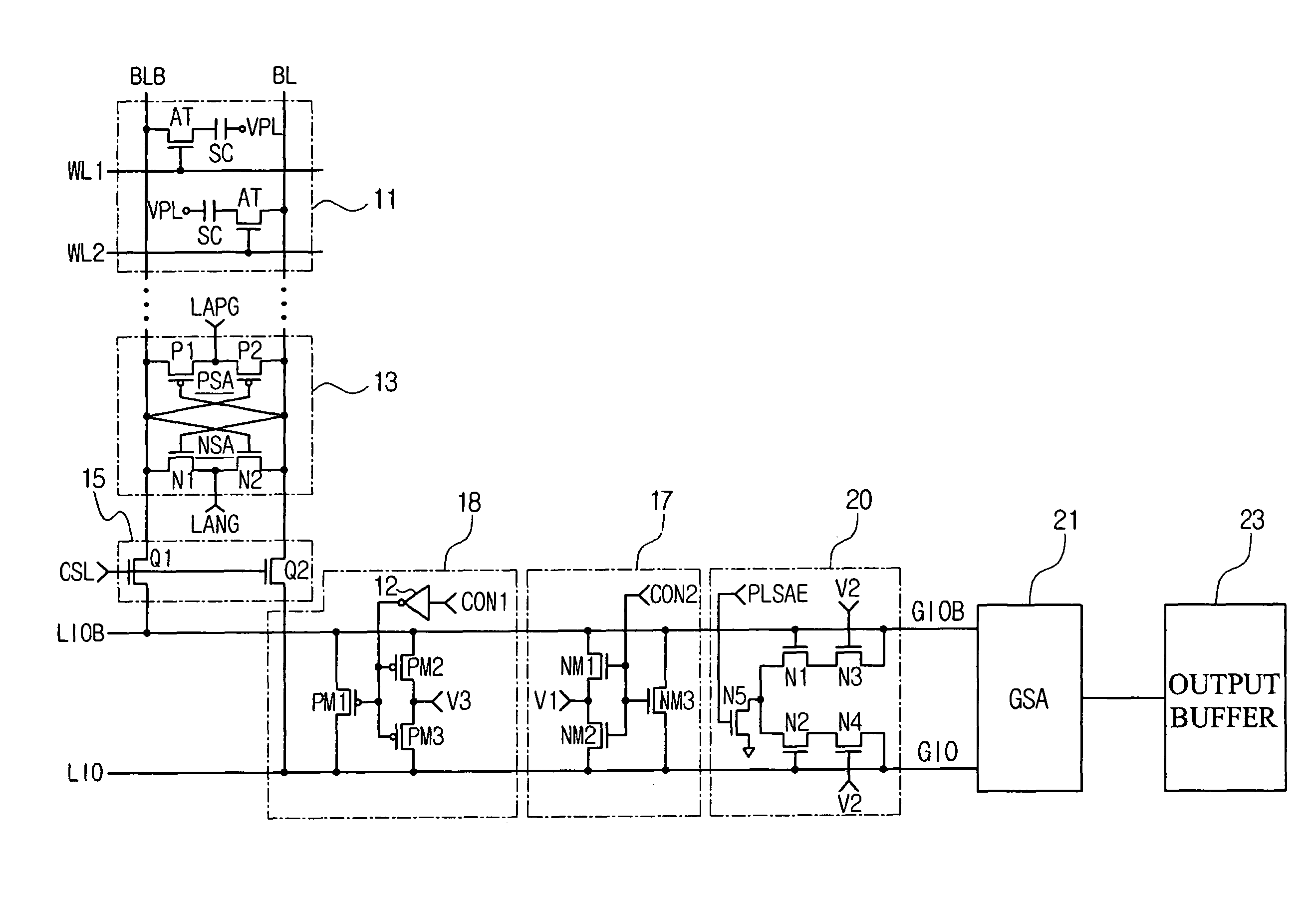
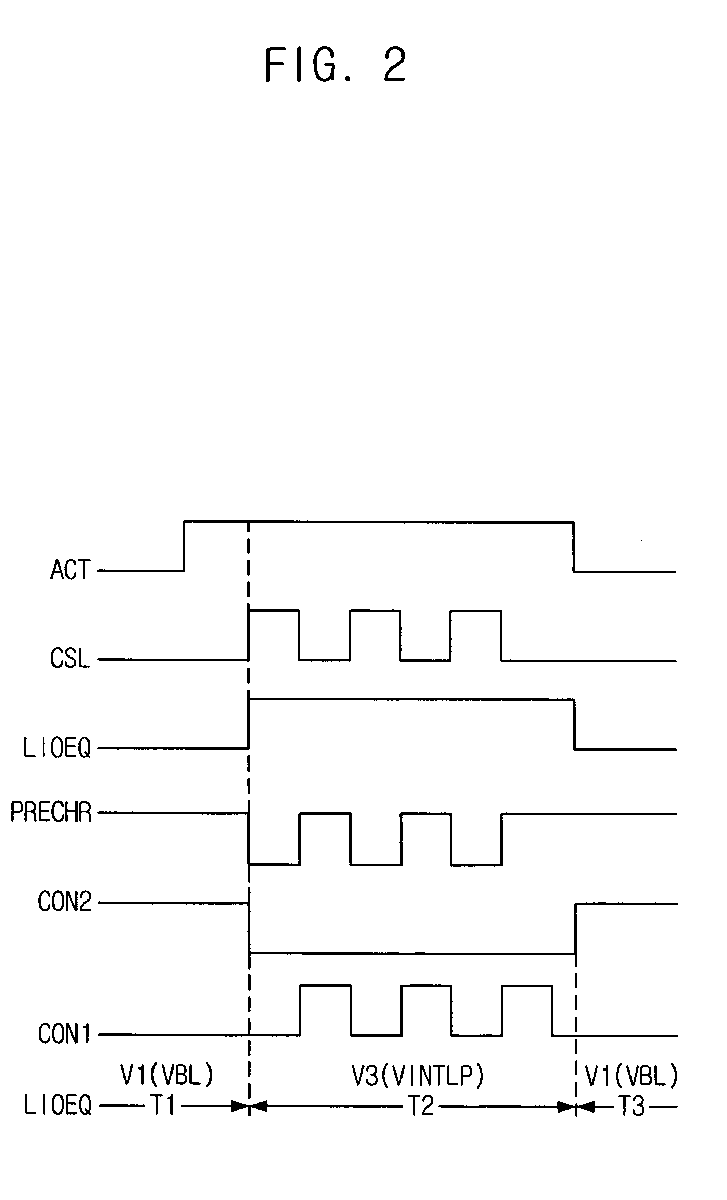
[0033]Korean Patent Application No. 10-2009-0019324, filed on Mar. 6, 2009, in the Korean Intellectual Property Office, and entitled: “Semiconductor Memory Device Having Improved Local Input / Output Line Precharge Scheme,” is incorporated by reference herein in its entirety.

[0034]Exemplary embodiments will now be described more fully hereinafter with reference to the accompanying drawings; however, they may be embodied in different forms and should not be construed as limited to the embodiments set forth herein. Rather, these embodiments are provided so that this disclosure will be thorough and complete, and will fully convey the scope of the invention to those skilled in the art. More particularly, exemplary embodiments of semiconductor memory devices capable of minimizing or preventing bit line disturbance, reducing power consumption, and / or achieving a low-voltage and high-speed operation according will be described with reference to the accompanying drawings. It will be understoo...


PUM


Abstract

A data path circuit of a semiconductor memory device includes: a bit line sense amplifier driven by a first power supply voltage; a local input / output line sense amplifier; a column selecting unit operatively connecting a pair of bit lines connected to the bit line sense amplifier and a pair of local input / output lines connected to the local input / output line sense amplifier in response to a column selection signal; and a local input / output line precharge unit precharging the pair of local input / output lines with a second power supply voltage different from the first power supply voltage during a period for which the column selection signal is in an inactive state.

Description

BACKGROUND[0001]1. Field[0002]Embodiments relate to a semiconductor memory device. More particularly, embodiments relate to a data path circuit of a semiconductor memory device, such as a dynamic random access memory.[0003]2. Description of the Related Art[0004]In recent years, the processing speed and the degree of integration of semiconductor memory devices, such as dynamic random access memories, have been increased to meet user demands. A dynamic random access memory (DRAM) device including one access transistor and one storage capacitor as a unit memory cell is generally used as a main memory of an electronic system.[0005]During the read operation of a DRAM, a bit line sense amplifier may sense and amplify data stored in the memory cells on a pair of bit lines. Then, when a column selection line (hereinafter, referred to as a CSL) signal is activated, the amplified data may be transmitted to a pair of local input / output lines. The data transmitted to the pair of local input / out...

Claims


Application Information

Patent Timeline
Patent Type & Authority Patents(United States)
IPC IPC(8): G11C7/00
CPCG11C7/1048G11C11/4096
Inventor MOON, JONG-HOJANG, SEONG-JIN
Owner SAMSUNG ELECTRONICS CO LTD
Why Eureka
Try Eureka