Method for creating electrically testable patterns

a technology of electrical test patterns and electrical testing, applied in the direction of originals for photomechanical treatment, semiconductor/solid-state device testing/measurement, instruments, etc., can solve the problems of relatively simple current electrical test patterns and not fully representing the range of sensitive patterns

Inactive Publication Date: 2012-07-10
GLOBALFOUNDRIES INC
View PDF14 Cites 1 Cited by
  • Summary
  • Abstract
  • Description
  • Claims
  • Application Information

AI Technical Summary

Benefits of technology

[0011]According to one aspect of the invention, a method is provided for designing an electrical test pattern comprising the steps of providing a chip design comprising a chip layout of a first layer of features to be printed; identifying a critical site in the chip layout; identifying at least one electrical test feature of the chip layout adjacent the critical site, the at least one electrical test feature having at least one electrical characteristic that will be significantly modified if a printing failure occurs at the critical site; defining a region of influence (ROI) around the critical site such that printing of the critical site will not be influenced more than a predetermined critical site tolerance by the absence of features outside the ROI; defining at least one feed line electrically connected to said at least one electrical test feature to enable testing of said at least one electrical characteristic; defining a trim region outside of the ROI such that the absence of any feature of the chip layout located outside of the trim region will not substantially, within a predetermined ROI tolerance, affect the printed dimensions of any feature within the ROI; and deleting all features, other than said at least one feed line and said at least one electrical test feature, located outside of said trim region to form a customized electrical test pattern.

Problems solved by technology

Patterning densely spaced geometries, as for example, a static random access memory (SRAM) cell and other process sensitive 2-D geometries for increasingly smaller technologies, e.g. 65 nm technologies or smaller, presents a major challenge.
However, current electrical test patterns are relatively simple, such as serpentine or comb structures, and have been limited in the range of geometries covered, and may not fully represent the range of sensitive patterns that may occur in an actual chip design.

Method used


Image

  • Method for creating electrically testable patterns
  • Method for creating electrically testable patterns
  • Method for creating electrically testable patterns

Examples


Embodiment Construction

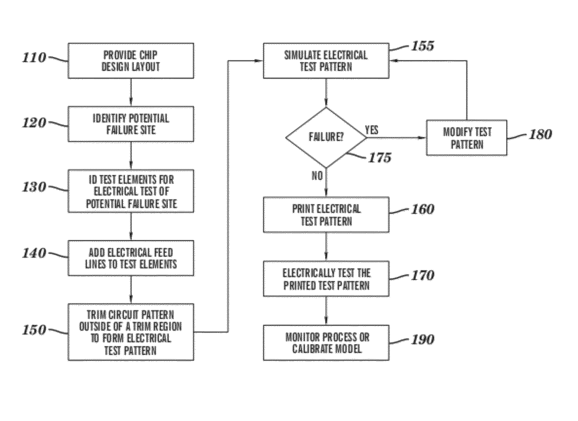
[0034]This invention presents a method for designing customized electrically testable patterns that more accurately represent the most sensitive structures arising from an actual chip design. Such customized electrical test patterns may be used to monitor any lithographic process used to transfer (or equivalently, print) a chip layout to a wafer. The term “lithographic process” as used and referred to herein, includes, without limitation, any pattern transfer process, such as forming a resist image, forming implants, performing a patterned etch, etc.

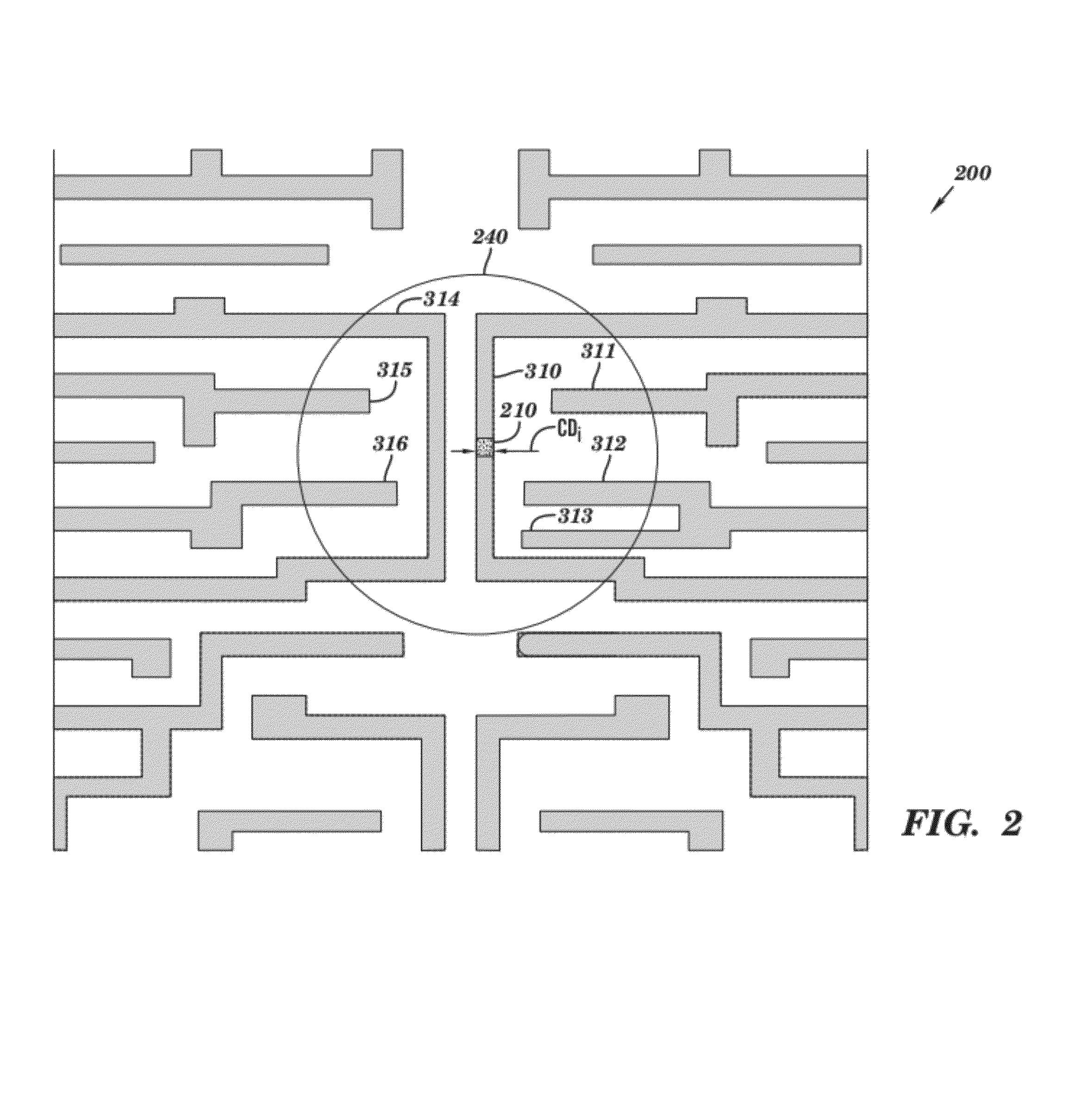
[0035]One embodiment of a method for designing an electrical test pattern, in accordance with the invention, is illustrated in FIG. 1. First, a chip layout of interest is provided (Block 110). The chip layout may be one of several layers of a chip design, containing a layout of polygons that represent critical features of the chip that are to be printed. Next, potential failure sites, or critical sites, are identified in the chip layout,...


PUM


Abstract

The present invention provides a method and computer program product for designing an electrically testable pattern that is based on patterns derived from the desired chip layout to be printed. Such electrical test patterns are based on the features within a region of influence around critical sites. The critical sites may be identified, for example, by processing the chip layout through an OPC verification tool that flags potential failure sites. The electrical test pattern is formed from features within an region of influence (ROI) around the critical site, and also include electrical feed lines at terminal ends of one or more features having an electrical characteristic that is sensitive to changes in the printed environment of the critical site. The feed lines may be locate on the same or a different layer than the critical site, depending on the chip design. The electrical pattern is further defined by retaining features within a second trim region such that the printed features within the ROI are not substantially modified by the absence of features outside the second trim region.

Description

FIELD OF THE INVENTION[0001]The present invention broadly relates to the design of integrated circuits, particularly to the design of lithographic masks, and more particularly to improvements in creating electrically testable patterns for use in monitoring lithographic processes and calibrating lithographic models used in mask design processes such as optical proximity correction (OPC) or in OPC Verification.BACKGROUND[0002]In the manufacture of integrated circuits, photolithographic processes are commonly used, in which a wafer is patterned by projecting radiation through a patterned mask to form an image pattern on a photo sensitive material, referred to as a photoresist, or simply resist. The exposed resist material is developed to form openings corresponding to the image pattern, and then the pattern is transferred to the wafer substrate by methods such as etching, as known in the art.[0003]The basic lithography system consists of a light source, a photomask containing the patte...

Claims


Application Information

Patent Timeline
Patent Type & Authority Patents(United States)
IPC IPC(8): G06F17/50
CPCG03F1/36G03F1/44G03F1/84H01L22/34H01L2924/0002H01L2924/00
Inventor BRUCE, JAMES A.CONRAD, EDWARD W.SMOLINSKI, JACEK G.
Owner GLOBALFOUNDRIES INC
Why Eureka
Try Eureka