Electronic circuit with cascode amplifier

a cascode transistor and amplifier technology, applied in amplifiers, amplifiers with semiconductor devices only, amplifiers with semiconductor devices, etc., can solve problems such as cascode transistor breakdown risk, and achieve the effect of improving circuit efficiency

Active Publication Date: 2012-07-24
TELEFON AB LM ERICSSON (PUBL)
View PDF7 Cites 17 Cited by
  • Summary
  • Abstract
  • Description
  • Claims
  • Application Information

AI Technical Summary

Benefits of technology

[0007]Among others it is an object to improve the efficiency of a circuit with a cascode amplifier.
[0009]In an embodiment the capacitive voltage divider is configured to maximize the voltage at the drain of the cascode transistor at which break-down of any transistor of the amplifier may occur. In an embodiment the bias voltage supply circuit is configured to maximize power efficiency of the amplifier. The capacitive voltage divider and the bias voltage supply circuit may optimize the breakdown voltage and the efficiency at the same time.
[0010]In an embodiment the capacitive voltage divider applies fraction of the drain voltage of the cascode transistor to its gate. In an embodiment this fraction is smaller than a ratio between the average gate voltage of the cascode transistor supplied by the bias voltage supply circuit and the average drain supply voltage. Thus, it is possible to use an amplifying transistor that has a lower breakdown voltage than the cascode transistor, to provide for improved amplifier gain.
[0011]In an embodiment the bias voltage supply circuit comprises a resistive voltage divider coupled between the drain of the cascode transistor and the power supply reference connection with a divided voltage output coupled to the gate of the cascode transistor; and an offset voltage source coupled to the gate of the cascode transistor. Thus a simple way of generating the average bias is realized. It has been found that optimal efficiency can substantially be achieved by such a circuit.

Problems solved by technology

This gives rise to a risk of cascode transistor breakdown.

Method used


Image

  • Electronic circuit with cascode amplifier
  • Electronic circuit with cascode amplifier
  • Electronic circuit with cascode amplifier

Examples


Embodiment Construction

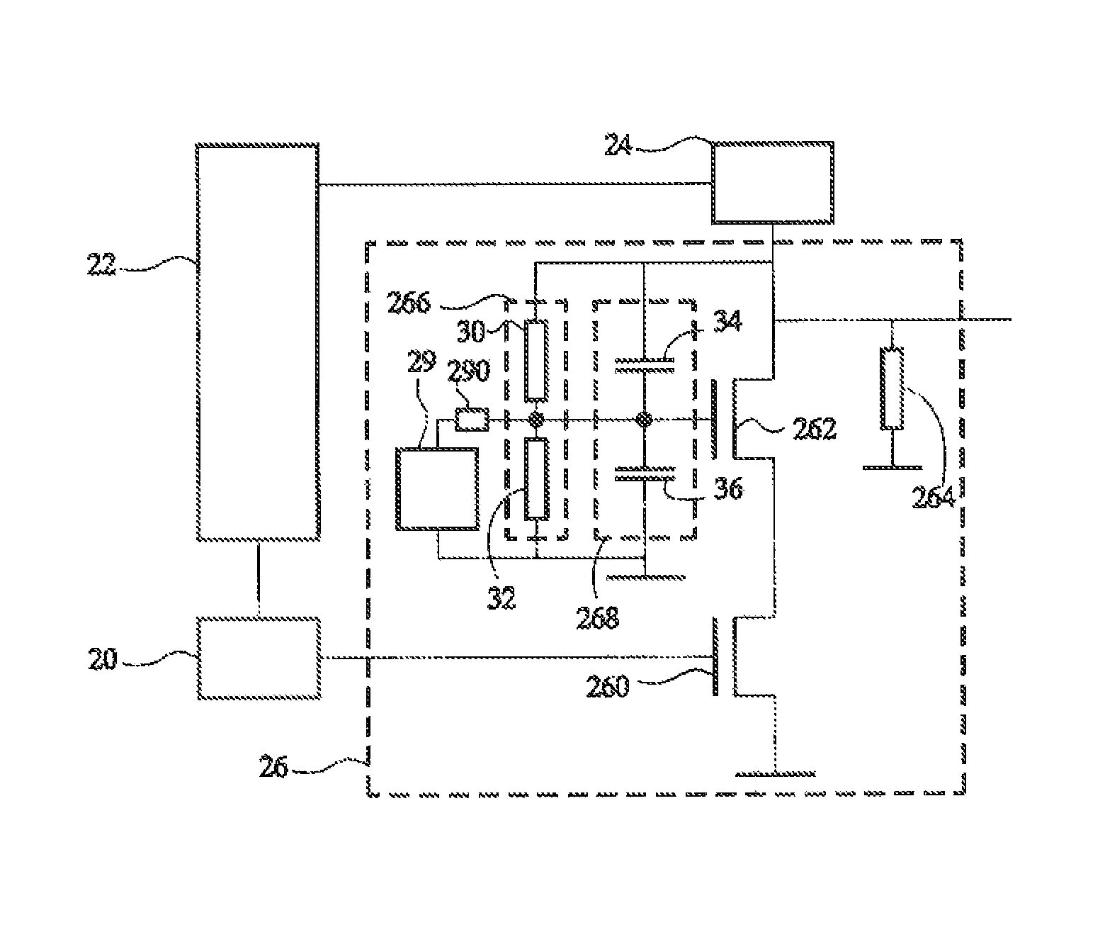
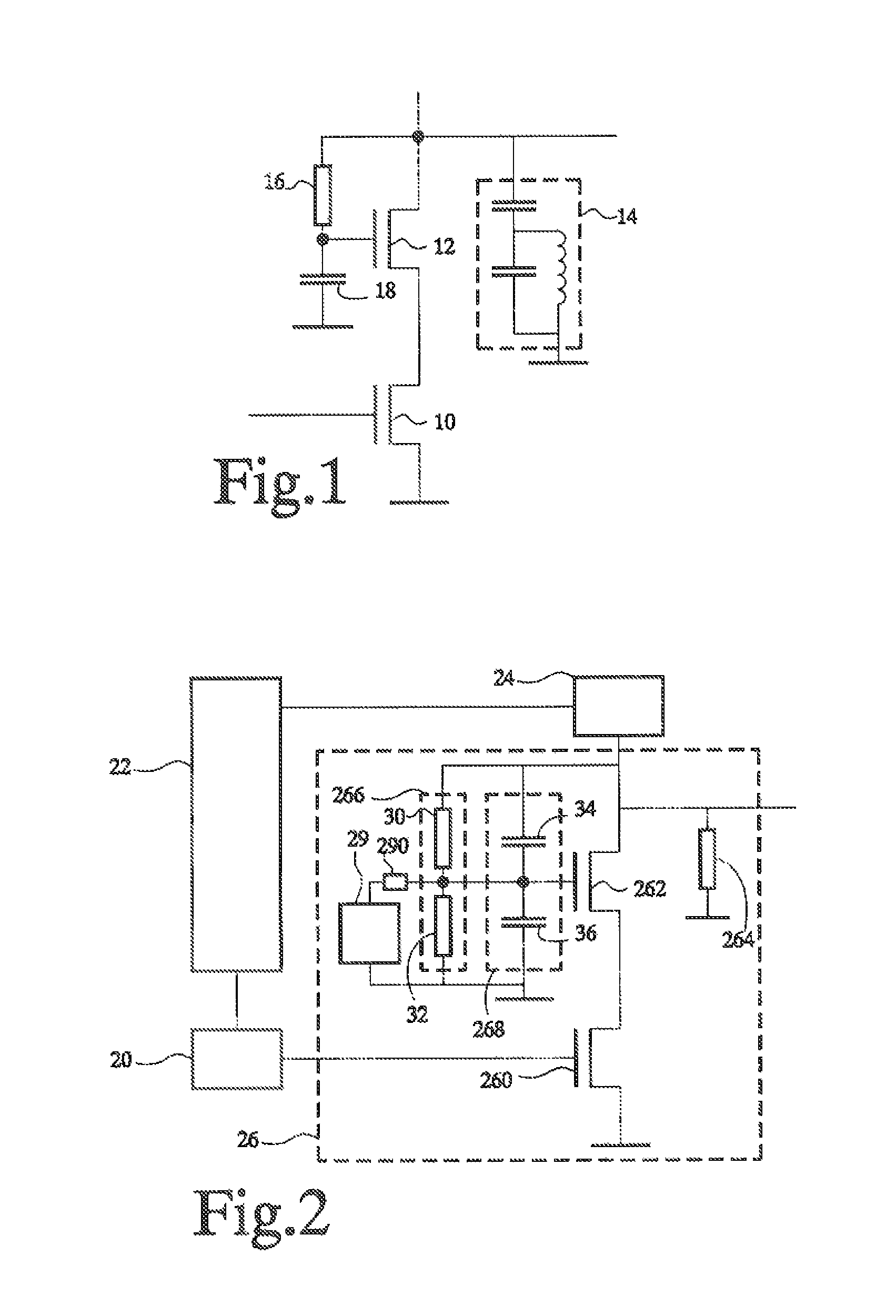
[0019]FIG. 2 shows an electronic circuit comprising an RF signal source 20, a modulation source 22, a voltage control circuit 24 and an amplifier 26. Modulation source 22 has a first output coupled to phase and / or frequency control input of RF signal source 20. RF signal source 20 has an RF output coupled to a signal input of amplifier 26. Modulation source 22 has a second output coupled to a control input of voltage control circuit 24. Voltage control circuit 24 has a voltage output coupled to a supply voltage input of amplifier 26. In operation modulation source 22 uses RF signal source 20 to modulate the phase and / or frequency of the RF signal and modulation source 22 uses voltage control circuit 24 and amplifier 26 to realize a modulation of the amplitude of the RF signal, by varying a supply voltage that is applied to amplifier 26. Voltage control circuit 24 is configured to control the average supply voltage of amplifier 26, while allowing RF voltage swing at the supply input ...


PUM


Abstract

An electronic circuit has an amplifier with an amplifying transistor and a cascode transistor. A capacitive voltage divider applies a fraction of an RF signal swing from the drain of the cascode transistor to the gate of the cascode transistor, the fraction being determined by a ratio between capacitance values. In addition a bias voltage supply circuit is provided. The bias voltage supply circuit is configured to define a relation between an average gate voltage of the cascode transistor and an average drain supply voltage at the drain of the cascode transistor. This relation increases the average gate voltage with increasing average drain voltage, and the relation provides a non zero average gate voltage when extrapolated to zero average drain supply voltage.

Description

CROSS-REFERENCE TO RELATED APPLICATION(S)[0001]The present application claims priority under 35 U.S.C. §365 to International Patent Application No. PCT / EP2008 / 065231 filed Nov. 10, 2008, entitled “ELECTRONIC CIRCUIT WITH CASCODE AMPLIFIER”. International Patent Application No. PCT / EP2008 / 065231 claims priority under 35 U.S.C. §365 and / or 35 U.S.C. §119(a) to European Patent Application No. 07120318.6 filed Nov. 9, 2007 and which are incorporated herein by reference into the present disclosure as if fully set forth herein.FIELD OF THE INVENTION[0002]The invention relates to a circuit with an amplifier that includes a cascode transistor.BACKGROUND OF THE INVENTION[0003]An amplifier with a cascode transistor is known from an article titled “A 2.4-GHz 0.18- m CMOS Self-Biased Cascode Power Amplifier”, by Tirdad Sowlati, and Domine M. W. Leenaerts and published in the IEEE Journal of Solid-State Circuits, vol. 38, no. 8, Aug. 2003. This amplifier has a resonant load circuit that has the ...

Claims


Application Information

Patent Timeline
Patent Type & Authority Patents(United States)
IPC IPC(8): H03F1/22
CPCH03F1/223H03F1/0266H03F3/45188H03F2200/18
Inventor HEIJDEN, MARK PETERLEENAERTS, DOMINICUSAPOSTOLIDOU, MELINA
Owner TELEFON AB LM ERICSSON (PUBL)
Why Eureka
Try Eureka