Semiconductor device

a technology of semiconductor devices and semiconductors, applied in semiconductor devices, semiconductor/solid-state device details, electrical apparatus, etc., can solve problems such as large mounting area, electrical property degradation, and electrical property degradation, and achieve the effect of efficiently performing wiring at the time of mounting

Inactive Publication Date: 2012-07-31
RENESAS ELECTRONICS CORP
View PDF19 Cites 11 Cited by
  • Summary
  • Abstract
  • Description
  • Claims
  • Application Information

AI Technical Summary

Benefits of technology

[0014]A purpose of the present invention is to improve the characteristics of a semiconductor device including the semiconductor chip which has a power transistor, and the semiconductor chip which has a circuit for a drive which drives the power transistor.
[0016]A purpose of the present invention is to make the structure of a semiconductor device able to perform the wiring at the time of mounting efficiently.

Problems solved by technology

When the semiconductor chip which has a power transistor, and the semiconductor chip which has a circuit for a drive which drives this power transistor are mounted in another package, respectively, and these packages are mounted in a wiring substrate etc., there is a problem that a mounting area becomes large or an electrical property deteriorates.
In this case, depending on the wiring layout on a wiring substrate, a wire length becomes long, and the problem of leading to degradation of an electrical property occurs.

Method used


Image

  • Semiconductor device
  • Semiconductor device
  • Semiconductor device

Examples


embodiment 1

[0057](Embodiment 1)

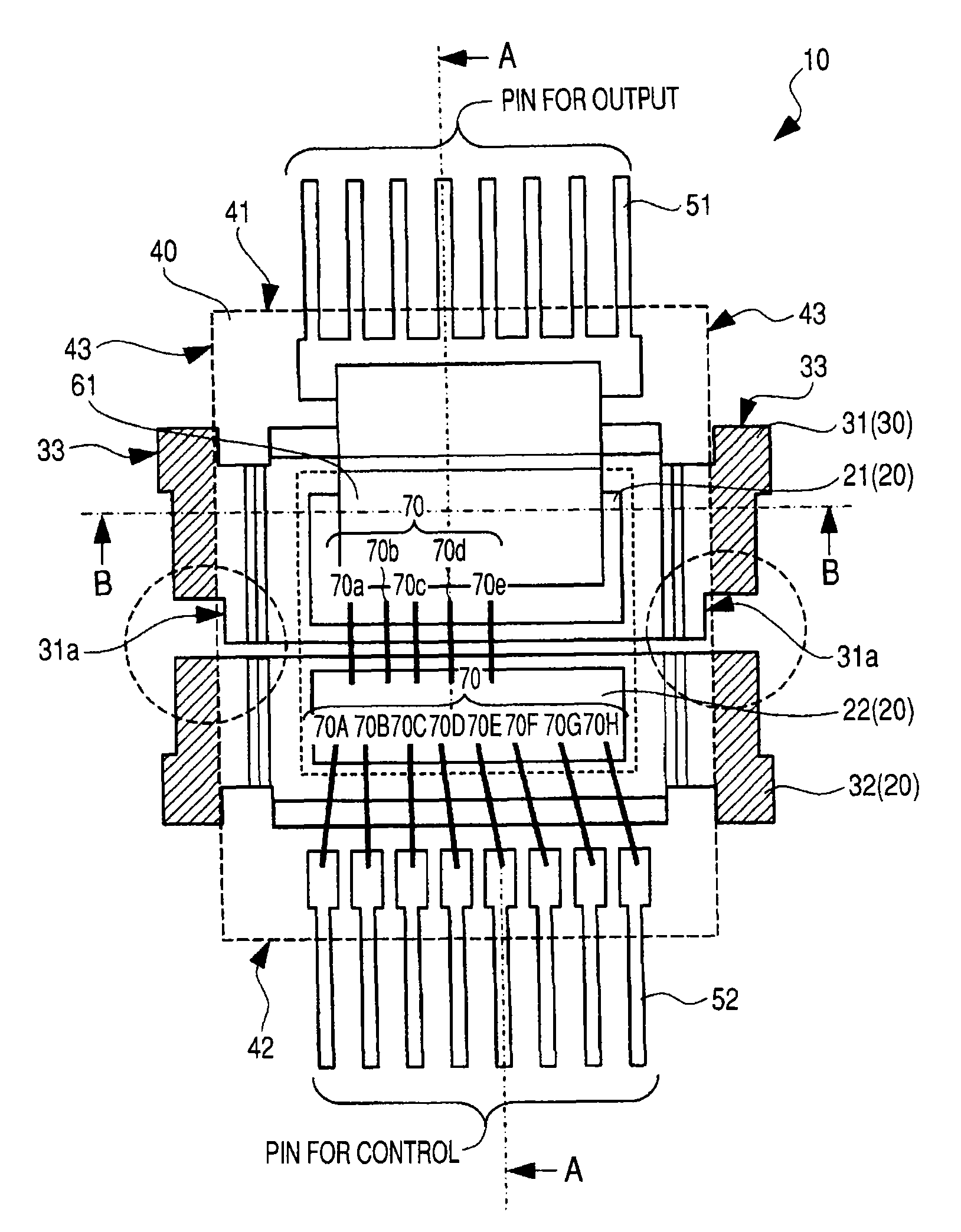
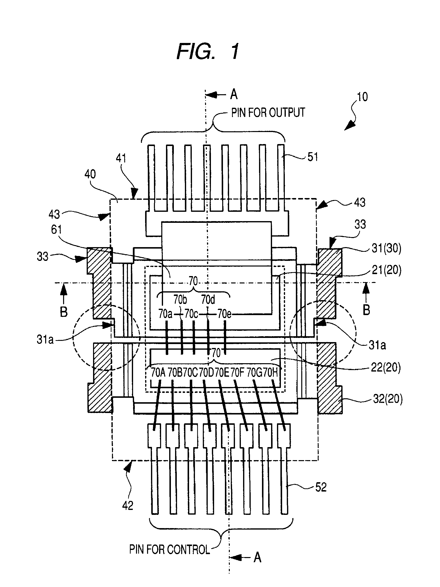
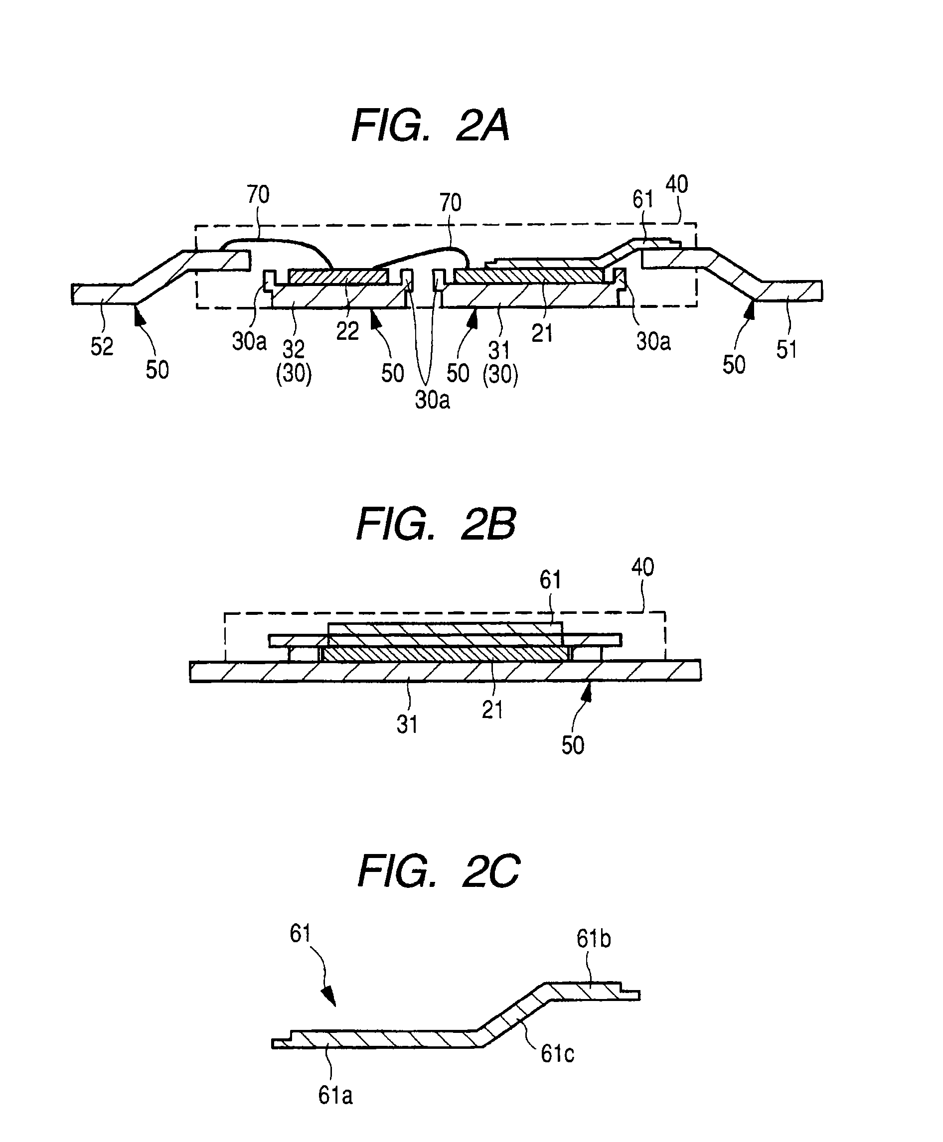
[0058]FIG. 1 is a plan view showing schematically an example of the entire configuration of the semiconductor device of the 1 embodiment of the present invention. FIG. 2A is a cross-sectional view showing schematically a state that the A-A line of FIG. 1 cut, FIG. 2B is a cross-sectional view showing schematically a state that the B-B line cut, and FIG. 2C is a cross-sectional view showing the structure of a flat electrode. FIG. 3 is a cross-sectional view showing the appearance of a die pad schematically. FIG. 4 is a section explanatory diagram showing the clearance between die pads. FIG. 5 (a) is a cross-sectional view showing schematically the state of cutting by the A-A line at the time of forming the semiconductor device of structure of being shown in FIG. 1 using the lead frame of the structure whose thickness of a die pad part is thicker than a lead, and (b) is a cross-sectional view showing the state of cutting by a B-B line. FIG. 6 is a cross-sectional v...

embodiment 2

[0129](Embodiment 2)

[0130]This embodiment explains the case where the metal mold used when division structure of the die pad is done can perform a mold, even the die pad of one-sheet structure by forming the cut of first end face 31a deeply, as the Embodiment 1 described.

[0131]With the division structure of die pad 30, it is important like the above to form a cut of first end face 31a deeply. However, even if it uses the metallic mold used at the time of this division structure, sealing body 40 suitable enough can be formed by applying to die pad 30 of one-sheet structure.

[0132]For example, although division structure of the die pad 30 is not done when shown in FIG. 11, first end face 31a is deeply formed so that it may enter inside sealing body 40. Chip 21a is mounted on this die pad 30, and the source electrode is connected with flat electrode 61 to lead 50a formed in the pin for an output etc. A gate electrode is also connected to lead 50b not with wire connection but with flat e...

embodiment 3

[0134](Embodiment 3)

[0135]This embodiment explains other examples by which division structure of the die pad 30 is not done like the Embodiment 2. As shown in FIG. 12A, the case where chip 21a which is MOSFET, for example is mounted on die pad 30 can be mentioned. Also by this case, since first end face 31a of die pad 30 is deeply formed as the metallic mold sealing described, resin leakage can be prevented at the time of a mold, and sealing body 40 can be formed in sufficient accuracy.

[0136]As for chip 21a, the source electrode is connected with lead 50a by flat electrode 61 with this structure. By wire bonding, the gate electrode is connected to lead 50b with wire 70. Al or Au is used for wire 70, for example. In this structure, using the same lead frame 50, leads 50a and 50b and die pad 30 are formed so that board thickness may become the same.

[0137]The case where lead frame 50 with same board thickness was used was shown in FIGS. 12B and 12D. Even if it uses lead frame 50 in whi...


PUM


Abstract

It is made for the layout of the mounting wiring at the time of mounting to become efficient by changing the structure of a semiconductor device.A first chip is mounted on a first die pad, and a second chip is also mounted on a second die pad. A first die pad and a second die pad do division structure in parallel to the first side and second side of sealing body 40. As a result, the pin for an output from a first chip and the pin for control of the circuit for a drive can make it able to project from a counter direction, and can set the wiring layout at the time of mounting as the minimum route.

Description

CROSS-REFERENCE TO RELATED APPLICATION[0001]The present application claims priority from Japanese patent application No. 2006-234061 filed on Aug. 30, 2006, the content of which is hereby incorporated by reference into this application.[0002]1. Field of the Invention[0003]The present invention relates to semiconductor technology, and particularly relates to an effective technology in the application to the semiconductor device which includes the semiconductor chip which has a power transistor, and the semiconductor chip which has a circuit for a drive which drives the power transistor in one package.[0004]2. Description of the Background Art[0005]The technology explained below was examined by the present inventor when completing the present invention, and the outline is as follows.[0006]Some transistors are called the power transistor which can send big current. Especially this power transistor is used in the circuit for motor drives used by car etc. in recent years, and the demand ...

Claims


Application Information

Patent Timeline
Patent Type & Authority Patents(United States)
IPC IPC(8): H01L23/495
CPCH01L21/565H01L23/49503H01L23/49524H01L23/49562H01L23/49575H01L24/32H01L24/33H01L24/36H01L24/40H01L24/49H01L24/73H01L24/91H01L24/29H01L24/05H01L24/34H01L24/45H01L2224/45124H01L2224/45144H01L2224/48091H01L2224/48137H01L2224/48247H01L2224/48463H01L2224/4847H01L2224/49171H01L2224/49175H01L2224/73219H01L2224/73221H01L2224/73265H01L2924/01002H01L2924/01004H01L2924/01005H01L2924/01013H01L2924/01014H01L2924/01015H01L2924/01022H01L2924/01028H01L2924/01029H01L2924/01047H01L2924/0105H01L2924/01074H01L2924/01078H01L2924/01079H01L2924/01082H01L2924/13055H01L2924/13091H01L2224/32257H01L24/48H01L2924/01006H01L2924/01033H01L2924/014H01L2224/32245H01L2924/0132H01L2924/0133H01L2224/29111H01L2224/29139H01L2224/04042H01L2924/1305H01L2924/00014H01L2924/00H01L2924/181H01L2224/40095H01L2224/40245H01L2924/12042H01L2224/83801H01L2224/8385H01L2224/84801H01L24/84H01L2224/2612H01L2924/00012H01L2224/37099
Inventor KOIKE, NOBUYAFUJIKI, ATSUSHIKIDO, NORIOSATO, YUKIHIRONAKAMURA, HIROYUKI
Owner RENESAS ELECTRONICS CORP
Why Eureka
Try Eureka