Methods and apparatus for reducing defect bits in phase change memory

a phase change memory and defect bit technology, applied in the field of memory devices, can solve the problems of bit errors, rapid decrease in resistance, bit errors, etc., and achieve the effects of high resistance reset state, high current, and increased amount of amorphous phase materials

Active Publication Date: 2012-08-07
MACRONIX INT CO LTD +1
View PDF426 Cites 15 Cited by
  • Summary
  • Abstract
  • Description
  • Claims
  • Application Information

AI Technical Summary

Benefits of technology

[0019]If the I-V behavior indicates that the memory cell may be a defect cell, techniques described herein include applying an additional high current operation to establish the high resistance reset state. The additional high current operation can increase the amount of amorphous phase material within the active region, for example by having a higher pulse amplitude, and / or a shorter pulse tail, than that of the initial high current operation. As a result, a memory cell which is a defect cell following the initial high current operation can be properly reset by the additional high current operation. As a result, the techniques described herein overcome the data retention issues of defect cells caused by having a small amount of amorphous phase material, and thus extend the useful life of the memory cells. In addition, since the additional high current operation is applied only if the memory cell is a defect cell, issues such as over-resetting of memory cells which have been properly reset by the initial high current operation are avoided.

Problems solved by technology

One problem arising in phase change memory devices involves data retention in the high resistance state 102.
As a result, when these memory cells (referred to herein as defect cells) are read the lower resistance state 100 will be detected, resulting in bit errors.
As a result, after a relatively short amount of time, a low resistance crystalline phase path can be formed through the active regions of these defect cells, resulting in bit errors.
Furthermore, because phase change memory resistance depends upon a number of factors, the memory cells which will experience a rapid decrease in resistance and are thus defect cells may not be identified based on their initial resistance value.
Since the phase change material undergoes a phase change as a result of heating, using unnecessarily high current levels can result in electrical and mechanical reliability problems for the memory cells.
These problems include the formation of voids at the phase change material / electrode interfaces due to mechanical stress caused by thermal expansion and material density changes during operation.
Additionally, using significantly higher current levels than necessary can result in problems such as localized heating sufficient to induce diffusion / reaction of electrode and phase change material, and / or cause compositional changes in the phase change material within the active region, resulting resistive switching degradation and possible failure of the memory cell.
Defect cells can also arise due to a persistently small retention time in the high resistance state 102 which develops during the life of the device.

Method used


Image

  • Methods and apparatus for reducing defect bits in phase change memory
  • Methods and apparatus for reducing defect bits in phase change memory
  • Methods and apparatus for reducing defect bits in phase change memory

Examples


Embodiment Construction

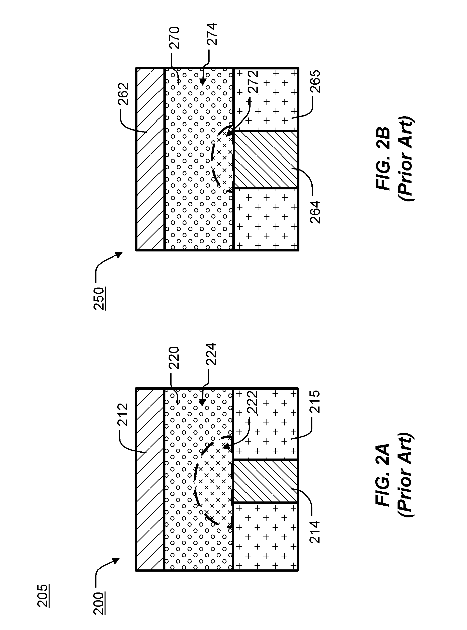
[0038]A detailed description of embodiments of the present invention is provided with reference to the FIGS. 2A-2B to 14A-14C.

[0039]FIGS. 2A-2B illustrates cross-sectional views of two prior art “mushroom type” memory cells 200, 250 in an array 205 that can include millions of memory cells. The first memory cell 200 includes a bottom electrode 214 extending through dielectric 215, a memory element 220 comprising a phase change material, and a top electrode 212 on the memory element 224. The bottom electrode 224 is coupled to a terminal of an access device (not shown) such as a diode or transistor, while the top electrode 212 is coupled to a bit line or can be part of a bit line. The bottom electrode 214 has a width less than the width of the top electrode 212 and memory element 220, establishing a small contact area between the memory element 220 and the bottom electrode 214 and a relatively large contact area between the memory element 220 and the top electrode 212.

[0040]In operati...


PUM


Abstract

Phase change memory devices and methods for operating described herein are based on the discovery that, following an initial high current operation applied to a phase change memory cell to establish the high resistance reset state, the current-voltage (I-V) behavior of the memory cell under different bias voltages can be used to detect if the memory cell is a defect cell having poor data retention characteristics.

Description

CROSS-REFERENCE TO RELATED APPLICATIONS[0001]This application claims the benefit of U.S. Provisional Application No. 61 / 220,515 titled “Methods for Reducing Defect Bits and Early Failure Bits in Phase Change Memory” filed 25 Jun. 2009, which is incorporated by reference herein.PARTIES TO A JOINT RESEARCH AGREEMENT[0002]International Business Machines Corporation, a New York corporation, and Macronix International Corporation, Ltd., a Taiwan corporation are parties to a Joint Research Agreement.BACKGROUND OF THE INVENTION[0003]1. Field of the Invention[0004]The present invention relates to memory devices based on phase change based memory material, including chalcogenide materials and other programmable resistive materials, and to methods for operating such devices.[0005]2. Description of Related Art[0006]Phase change based memory materials, like chalcogenide materials and similar materials, can be caused to change phase between an amorphous and a crystalline phase by application of ...

Claims


Application Information

Patent Timeline
Patent Type & Authority Patents(United States)
IPC IPC(8): G11C11/00
CPCG11C13/0004G11C13/004G11C2213/79G11C29/70
Inventor SHIH, YEN-HAOLEE, MING-HSIUWU, CHAO-ILUNG, HSIANG-LANLAM, CHUNG HONCHEEK, ROGERBREITWISCH, MATTHEW J.RAJENDRAN, BIPIN
Owner MACRONIX INT CO LTD
Why Eureka
Try Eureka