Check patentability & draft patents in minutes with Patsnap Eureka AI!

Wirelessly configurable memory device addressing

a memory device and wireless configuration technology, applied in the field of computing devices, can solve the problems of consuming a significant amount of power for transferring data via the traces and drivers, little ability to reconfigure the architecture, and increasing the complexity of the random access memory basic architecture,

Inactive Publication Date: 2012-08-07
AVAGO TECH WIRELESS IP SINGAPORE PTE
View PDF103 Cites 0 Cited by
  • Summary
  • Abstract
  • Description
  • Claims
  • Application Information

AI Technical Summary

Benefits of technology

Enables efficient and flexible memory configuration, reducing power consumption and heat generation while improving data access speeds, allowing for dynamic allocation of memory resources based on application needs.

Problems solved by technology

While a great many advances have been made in memory technology, once the architecture of a memory device is implemented on an IC, there is little ability to reconfigure the architecture.
In addition, as integrated circuit technology advances, the basic architecture of random access memory is increasing in complexity, capabilities, and size reduction.
As is known, the transferring of data via the traces and drivers consumes a significant amount of power, which produces heat, and consumes a relatively significant amount of die area.

Method used


Image

  • Wirelessly configurable memory device addressing
  • Wirelessly configurable memory device addressing
  • Wirelessly configurable memory device addressing

Examples


Embodiment Construction

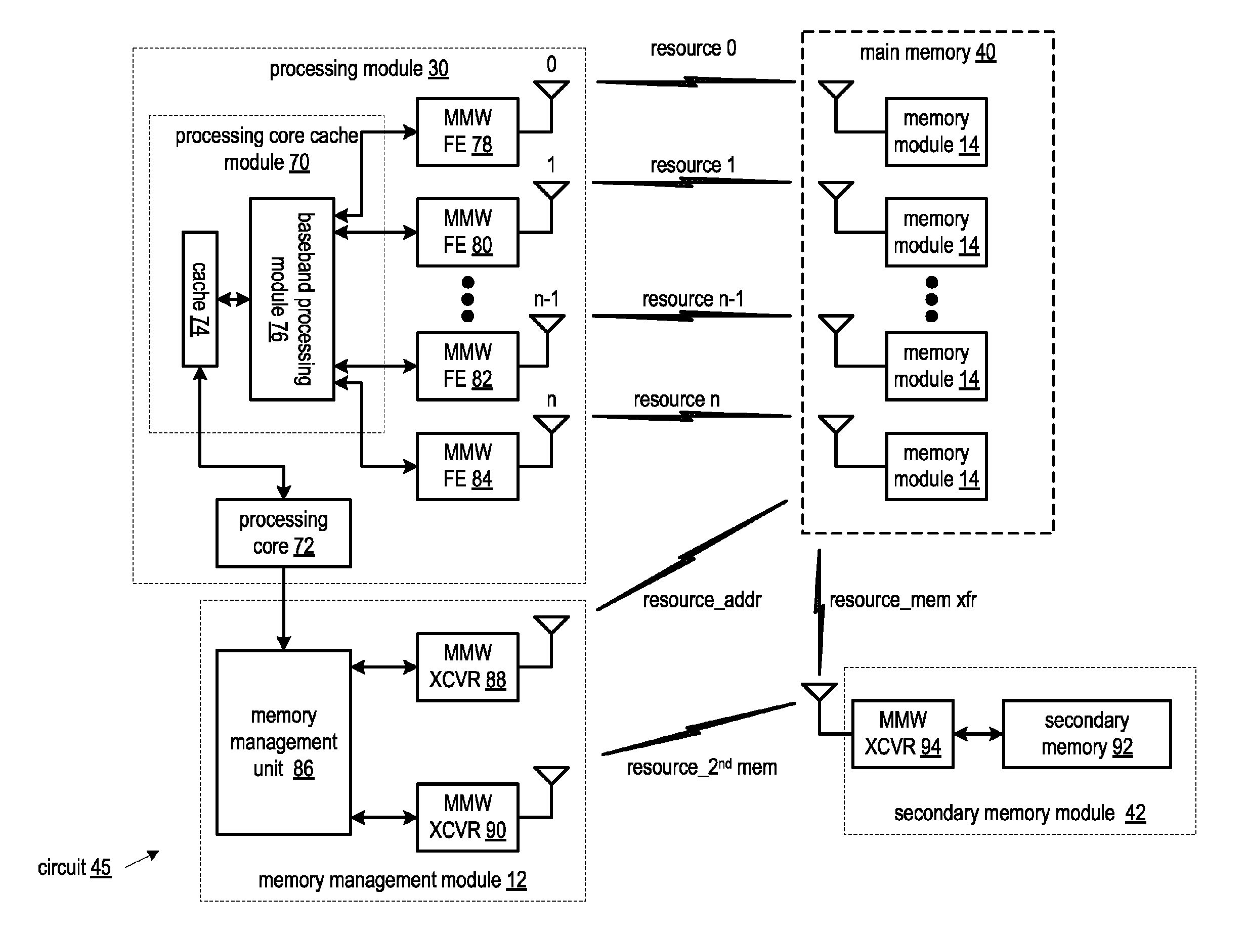
[0032]FIG. 1 is a schematic block diagram of an embodiment of a memory device 10 that includes a memory management module 12 and a plurality of memory modules 14. Each of the memory modules 14 includes a plurality of memory cells 16 and a millimeter wave (MMW) transceiver (XCVR) 18. The memory device 10 may be implemented on one or more dies of an integrated circuit (IC) and / or in one or more integrated circuits.

[0033]The MMW transceiver 18 includes a baseband processing module, a receiver section, and a transmitter section. The transmitter and receiver sections may share one or more antennas or each may have its own one or more antennas. The baseband processing module may include one or more processing devices, which may be a field programmable gate array, a programmable logic device, a state machine, logic circuitry, analog circuitry, digital circuitry, and / or any device that manipulates signals (analog and / or digital) based on hard coding of the circuitry and / or operational instr...


PUM


Abstract

A memory device includes a plurality of memory modules and a memory management module. A memory module of the plurality of memory modules includes a plurality of memory cells and a memory millimeter wave (MMW) transceiver. The memory management module determines a main memory configuration for at least some of the plurality of memory modules. The memory management module also determines physical addresses for the main memory configuration and determines a MMW communication resource table that includes an allocation mapping of one or more MMW communication resources to one or more of the at least some of the plurality of memory modules.

Description

[0001]This patent application is claiming priority under 35 USC §120 as a continuation in part patent application of co-pending patent applications:[0002]1. entitled COMPUTING DEVICE WITH HANDHELD AND EXTENDED COMPUTING UNITS, having a filing date of Feb. 6, 2008, and a Ser. No. 12 / 026,681;[0003]2. RF BUS CONTROLLER, having a filing date of Jan. 31, 2007, and a Ser. No. 11 / 700,285, issued on Feb. 14, 2012 as U.S. Pat. No. 8,116,294;[0004]3. entitled FLASH MEMORY WITH MILLIMETER WAVE HOST INTERFACE AND METHOD FOR USE THEREWITH, having a filing date of Jul. 31, 2007, and a Ser. No. 11 / 888,068, issued on Aug. 30, 2011 as U.S. Pat. No. 8,010,735; and[0005]4. entitled WIRELESSLY CONFIGURABLE MEMORY DEVICE, having a filing date of Aug. 30, 2008, and a Ser. No. 12 / 202,260, issued on May 8, 2012 as U.S. Pat. No. 8,175,108.STATEMENT REGARDING FEDERALLY SPONSORED RESEARCH OR DEVELOPMENT[0006]NOT APPLICABLEINCORPORATION-BY-REFERENCE OF MATERIAL SUBMITTED ON A COMPACT DISC[0007]NOT APPLICABLEBA...

Claims


Application Information

Patent Timeline
Patent Type & Authority Patents(United States)
IPC IPC(8): G06F12/00
CPCG06F12/0623G06F12/0646G06F12/1081G06F12/1009Y02B60/1225Y02D10/00
Inventor ROFOUGARAN, AHMADREZA REZAMARKISON, TIMOTHY W.
Owner AVAGO TECH WIRELESS IP SINGAPORE PTE
Features
  • R&D
  • Intellectual Property
  • Life Sciences
  • Materials
  • Tech Scout
  • Unparalleled Data Quality
  • Higher Quality Content
  • 60% Fewer Hallucinations
Learn More